

Building a PCB feels like solving a puzzle where mistakes cost time and money. Your frustration amplifies when schematics and layouts get mixed up. I’ve seen projects fail because this difference was overlooked. Let me save you from that headache.
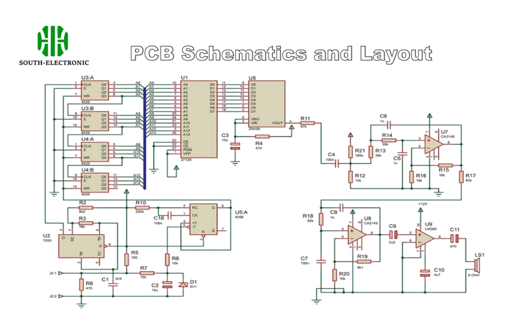
Schematics are conceptual blueprints showing component relationships through symbols, while layouts translate those concepts into physical board designs with actual copper traces and component placements.
Now you know the core distinction. But understanding alone won’t build your board. To succeed, you need practical workflows, error-spotting skills, and strategies for complex designs.
What’s the proven step-by-step workflow for PCB schematic design?
Dead-ended schematic work wastes hours and causes redesigns. Your deadline looms while you struggle with disorganized components. I nearly missed a product launch this way before refining my process.
Create schematics systematically: define requirements, draft block diagrams, place symbols, wire connections, validate with electrical rules, then export netlists. Keep component libraries updated throughout.
Build Your Foundation First
Start with core parameters:
- Board dimensions
- Power requirements
- Signal types (high-speed/digital/analog)
- Environmental factors
| Planning Stage | Key Questions | My Tip |
|---|---|---|
| Functionality | What signals will flow? | Group related circuits |
| Power Planning | What voltages are needed? | Calculate 20% extra capacity |
| Interface Needs | How will it connect externally? | Label all I/O clearly |
Without clear requirements, you risk rework. I once redesigned three times because current requirements were miscalculated. Next comes symbolic representation. Place every resistor, IC, and capacitor symbol according to functional groups. Connect them with nets showing electrical relationships. Always annotate components immediately – unlabeled parts cause chaos. Finally, run ERC (Electrical Rule Checks) before layout export.
What are the top PCB schematic errors?
Ever spent hours debugging a board only to find a schematic typo? I have. Silent errors wreck functional boards. Your prototype fails, deadlines vanish, and costs explode.
Mismatched symbol-footprint links cause unmanufacturable boards. Unconnected nets create open circuits. Inconsistent naming generates netlist conflicts.
Three Silent Killers of PCB Functionality
Footprint-Symbol Mismatch
The #1 manufacturing killer occurs when symbolic pins don’t match physical pad layouts. Verify every component individually:
- Compare datasheet pinouts
- Cross-check library entries
- Validate on 3D viewer
| Error Type | Detection Method | Prevention |
|---|---|---|
| Unconnected Pins | Net highlight in EDA tools | Enable ‘all pins wired’ rule |
| Power Conflicts | ERC voltage tier checks | Define power nets clearly |
| Naming Issues | Net comparison reports | Use prefix conventions |
During a medical device project, I discovered a voltage regulator symbol had inverted pins 30 minutes before production. You can’t catch errors without multiple verification passes. Electrical Rule Check (ERC) must run for unconnected pins, shorted nets, and output conflicts. But ERC alone isn’t enough. Manually spot-check high-risk areas like connectors and power sections.
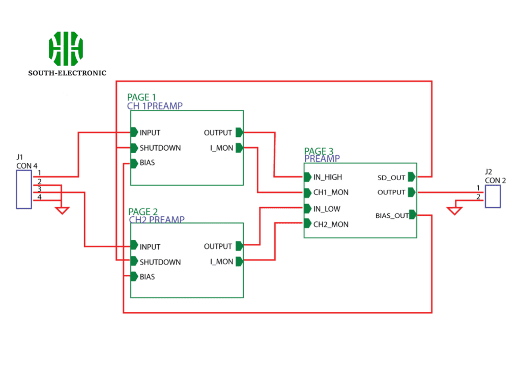
How to use hierarchical design for complex PCB schematics?
Overwhelmed by 500+ component schematics? Flat designs become unreadable spaghetti. I once debugged for days in a tangled schematic before adopting hierarchy.
Break complex circuits into functional modules: power section, sensors, controllers. Connect modules through ports. Manage cross-references for global nets.
Modular Building Strategy
Divide by Functionality
Group circuits performing specific tasks:
- Power subsystems
- Input/output blocks
- Processing cores
| Hierarchy Level | Purpose | Implementation |
|---|---|---|
| Top Sheet | Module connections | Ports and global nets |
| Sub-Schematics | Detailed circuit design | Component-level wiring |
| Repeat Blocks | Multi-channel circuits | Offsheet connectors |
Define clear interfaces between blocks using ports. For a recent IoT project, we separated WiFi, sensor processing, and battery circuits into modules. Four engineers collaborated without overlap. When module outputs change, only adjacent blocks need review. Keep top-level schematic clean – only connection lines between module ports. For recurring circuits (like sensor arrays), use repeated blocks. Update once and all instances sync automatically.
Conclusion
Schematics define logic, layouts shape physical reality. Mastering both prevents costly errors. Apply structured workflows daily – they transform complexity into clarity.

