
Mixing up packaging substrates and PCBs? They look similar but serve very different roles. Let’s break it down simply.
Packaging substrates connect chips to PCBs with ultra-high density; PCBs link larger components. They differ in density, use cases, and manufacturing precision.

I’ve worked with both in factories—seen teams misuse them. Let me show you their roles, differences, and why it matters. Mistakes here cost time and money; learn from mine.
What Do Packaging Substrates and PCBs Actually Do?
A client once used a PCB where a packaging substrate was needed. It failed. Their roles aren’t interchangeable.
Packaging substrates bridge chips and PCBs, aiding miniaturization and performance. PCBs connect larger components into functional circuits.

Core Functions
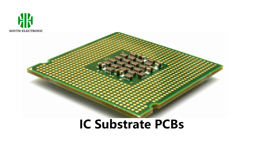
Packaging substrates sit between a chip and a PCB. They handle the chip’s tiny pins, translating them to a format PCBs can use. I used one in a smartphone chip—it let the 10,000-pin chip connect to a 1,000-pin PCB.
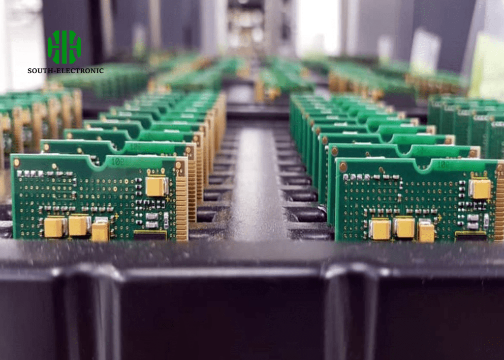
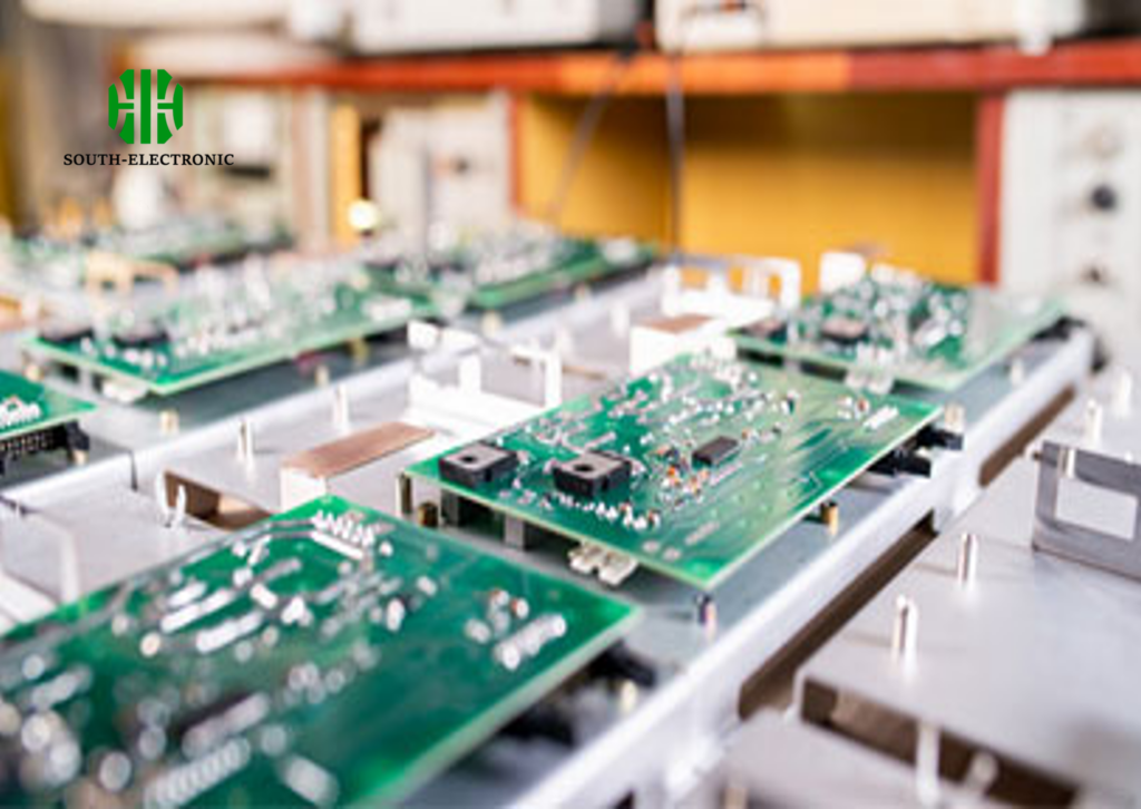
PCBs, on the other hand, connect bigger parts: resistors, capacitors, even packaged chips. A computer’s motherboard is a PCB. It links the CPU (in a package) to memory and ports.
Where They Fit in Packaging Layers
| Level | Packaging Substrates | PCBs |
|---|---|---|
| 1-2 level packaging | Used here (layers 2-3) | Rarely used |
| 2-3 level packaging | Seldom used | Used here (layers 3-5) |
In a smartwatch, the packaging substrate connects the main chip to a small PCB. That PCB then connects to the screen and battery. They’re a team—but with distinct jobs.
How Do Their Manufacturing Specs Compare?
I once tried using a high-end PCB for a chip—it couldn’t handle the tiny connections. The specs tell the story.
Packaging substrates need finer lines (≤25μm/25μm) vs. PCBs (≥50μm/50μm). They require more precision in production.
Line Width and Space
The biggest gap is in line width/space. A top-tier PCB might hit 50μm/50μm. But a standard packaging substrate does 25μm/25μm. For phone chips, I’ve used ones with 10μm/10μm—PCBs can’t touch that.
Production Methods
PCBs often use subtractive etching (removing copper). Packaging substrates need semi-additive (SAP) or modified semi-additive (MSAP) processes. These build up copper, allowing finer details.
| Spec | Packaging Substrate | High-End PCB |
|---|---|---|
| Line Width/Space | 25μm/25μm (standard) | 50μm/50μm (standard) |
| Process | SAP/MSAP | Subtractive etching |
| Hole Size | Smaller (laser-drilled) | Larger (mechanical drilling) |
Last year, we tried MSAP on a PCB for fun. It worked but cost 3x more—proving why PCBs stick to their methods.
Why Did Packaging Substrates Split From PCBs?
They started as one—so why did packaging substrates become their own thing? The answer lies in speed.
Packaging substrates split from PCBs in the 1980s due to chip advancements outpacing PCB density growth.
The 1980s Turning Point
Chips started shrinking fast with Moore’s Law. By the 1980s, large-scale ICs needed more pins in smaller spaces. PCBs couldn’t keep up. Their density improved, but not as fast as chips.
The Cost Factor
Making PCBs as dense as packaging substrates would be too expensive. It’s cheaper to have a specialized substrate connect the chip to a standard PCB.
I talked to an old engineer who worked in the 80s. He said they first tried beefing up PCBs, but yields dropped. Switching to dedicated substrates cut costs and boosted reliability. It was a no-brainer.
Today, chips with 10,000 pins need packaging substrates. A PCB would need huge size to match—and that defeats the “small” goal of electronics.
What Are Core and Coreless Packaging Substrates?
Confused by “core” and “coreless”? I was too until I used both. They’re two types with big trade-offs.
Core substrates have a central core board; coreless don’t. Coreless are thinner but prone to warping.
Core Substrates
They have a core board (like a thin PCB) with build-up layers on top/bottom. I used these for a tablet chip—they’re stable and easy to make. But they’re thicker.
Coreless Substrates
No core board—just build-up layers and copper pillars. They’re thinner, which is great for phones. But in my first test, 10% warped during production.
| Type | Pros | Cons | Best For |
|---|---|---|---|
| Core | Stable, easy to produce | Thicker | Larger devices (laptops) |
| Coreless | Thin, better signal speed | Warps easily | Small devices (phones) |
We switched to coreless for a 5G phone project. Added extra support during curing—warping dropped to 2%. It was worth it for the slimmer design.
Where Do They Each Get Used?
Ever pick up a device and wonder which board is which? They’re in almost everything—but in specific spots.
Packaging substrates go in chips (phones, GPUs). PCBs go in motherboards, backplanes, and smaller boards connecting components.
Packaging Substrate Uses
- Phone chips: Connects the main processor to the rest of the phone.
- GPUs: Handles high-speed data from the chip to the PCB.
- Wearables: Fits tiny chips into small spaces.
I helped design a fitness tracker. The packaging substrate here was smaller than a fingernail—connecting the sensor chip to a PCB the size of a coin.
PCB Uses
- Motherboards: In computers, linking the CPU, memory, and ports.
- Backplanes: In servers, connecting multiple PCBs.
- Car electronics: Connecting sensors, displays, and controllers.
A car’s infotainment system has a PCB connecting the touchscreen, speakers, and GPS. The GPS chip inside uses a packaging substrate to connect to that PCB.
Conclusion
Packaging substrates and PCBs work together but differ in density, roles, and specs. Know which to use—your design depends on it.

