Differences Between ICs and PCBs
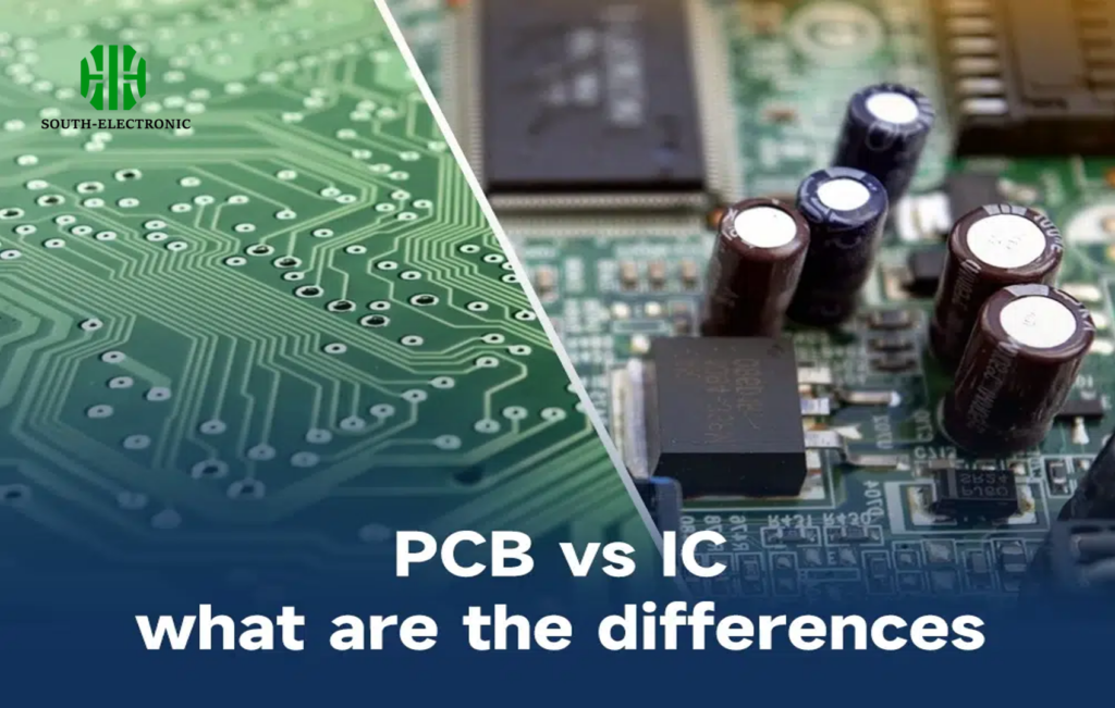
IC and PCB are two different but closely related components in electronic devices. They play different roles in the construction and functioning of electronic systems. Here are the main differences between ICs and PCBs:
Definition
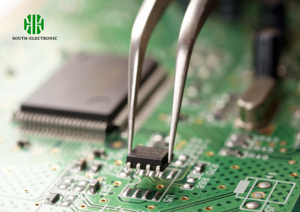
IC: An electronic device that integrates multiple electronic components (such as transistors, resistors, capacitors, etc.) on a tiny semiconductor chip. It performs specific circuit or system functions, such as data processing, signal amplification, logical operations, etc.
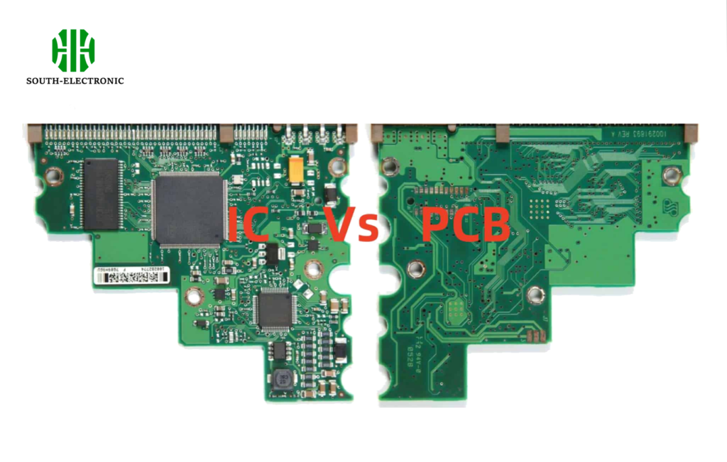
PCB: A substrate that serves as an electrical connection and mechanical support for electronic components. It is printed with conductive patterns to connect and fix electronic components to form a complete circuit or system.
Manufacturing process
IC: The manufacturing process involves complex semiconductor processes such as wafer preparation, photolithography, etching, doping, deposition, packaging, etc. These processes need to be carried out in a highly clean and precisely controlled environment.
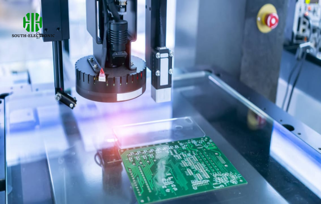
PCB: The manufacturing process includes steps such as substrate preparation, copper foil etching, drilling, electroplating, and assembly. Although precise control is also required, its complexity and technical requirements are lower than those of the IC manufacturing process.
Application
IC: It is the core component in electronic devices and is used to realize the functions of various circuits and systems. They are widely used in computers, mobile phones, home appliances, industrial control and other fields.
PCB: As the basic platform of electronic devices, it is used to connect and support IC and other electronic components. Almost all electronic devices require PCB to realize circuit connection and layout.
In the field of electronics, integrated circuits (ICs) and printed circuit boards (PCBs) are both basic components, but they serve different purposes and play different roles in electronic devices. Each layout plays a vital role in electronic products, but they apply to different aspects of the design and have varying scope and complexity. Understanding the differences between them is critical for anyone involved in electronics design and development. When comparing the layout scope of PCB (printed circuit board) and custom IC (integrated circuit), we need to consider multiple dimensions such as their physical form, design flexibility, application environment, etc.
PCB Layout: Broad Horizons
- Physical form:PCB is a fundamental component of electronic devices and the physical basis of electronic circuits. The physical form of a PCB includes its structure, materials, and layout, which are critical to its functionality and reliability.
- Design Flexibility:The design of PCB is highly flexible and can be customized according to different electronic system requirements. Its layout range is wide, it can accommodate a large number of electronic components and realize the interconnection between components through wiring.
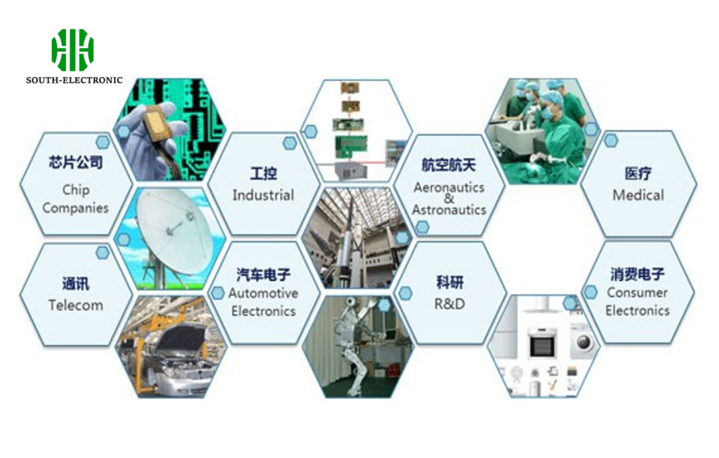
- Application Environment:Due to its relatively large size, PCB is often used in large electronic devices or systems. From consumer electronics to automobiles and telecommunications, PCB is an integral part of product development. In these systems, the PCB layout can range very widely to accommodate complex circuit structures and the placement of multiple components.
- Career and Industry Opportunities: Given its extensive application range, PCB design offers numerous career opportunities across various industries. From consumer electronics to automotive and telecommunications, PCB designers are integral to product development. The ability to work on diverse projects and the relative ease of iterating designs contribute to the broader scope of PCB layout.

Custom IC Layout: Specialized Expertise
- Physical form:A custom IC is a tiny three-dimensional structure that integrates a large number of tiny electronic components (such as transistors, resistors, capacitors, etc.) on a small block of semiconductor material (such as silicon). The degree of miniaturization of ICs far exceeds that of PCBs, and the scope of their internal layout is limited by the chip size and manufacturing process.
- Design Flexibility:Custom ICs can integrate millions or billions of transistors on a single chip, enabling much more complex and feature-rich designs compared to what can be achieved on a PCB. Circuits (ICs) allow for greater integration, higher performance, and more functionality to be packed into a smaller physical area compared to PCB-based designs.Although custom ICs have high integration and flexibility in circuit design, their layout range is mainly limited by the physical size and manufacturing process of the chip. Compared with PCBs, the layout range of ICs is relatively limited.
- Application Environment:Custom ICs are often used in small electronic devices such as mobile phones, laptops, micro drones, wearable devices, etc. due to their miniaturization and high integration. Although narrower in scope compared to PCB design, this position is essential to the development of cutting-edge technology and high-performance devices. Professionals in this field often work in a research and development environment, contributing to innovations in computing, telecommunications, and consumer electronics.
- Specialized Career Path: Careers in custom IC design are specialized and require advanced knowledge in semiconductor physics, electronic engineering, and design tools. While the scope is narrower compared to PCB design, the role is crucial for developing cutting-edge technologies and high-performance devices. Professionals in this field often work in research and development environments, contributing to innovations in computing, telecommunications, and consumer electronics.
Comparing the Scopes
Broadness of layout scope: From the perspective of physical form and design flexibility, the layout range of PCBs is wider than that of custom ICs. PCB can accommodate more electronic components and realize complex circuit structures through flexible wiring. The layout range of custom IC is limited by the physical size and manufacturing process of the chip.
PCB layout offers a wider range of applications with its wide range of applications and design flexibility. It provides the opportunity to work on a variety of projects and industries, making it an attractive option for those interested in a variety of electronic applications. On the other hand, custom IC layout is more specialized in scope, focusing on high performance and innovative designs. It requires deep technical expertise and is essential for chip-level technological advancements. The specialized nature of IC design may appeal to those interested in cutting-edge technology and complex problem solving.
Application scenarios: PCBs and custom ICs are each suited to different application scenarios. PCBs have a wider range of layouts in large electronic devices or systems; while custom ICs provide highly integrated solutions in small electronic devices. Both fields have strong industry demand, but they meet different needs.
PCB design is essential for creating and integrating electronic devices, while custom IC design is essential for pushing the boundaries of what technology can achieve. The choice between the two depends on whether a person prefers a wide range of applications or a deep dive into semiconductor technology.
Conclusion
PCB layout and custom IC layout represent two different but complementary aspects of electronic design. ICs provide the functionality, while PCBs provide the platform for interconnecting and supporting those ICs and other electronic components. Each aspect presents its own unique scope, challenges, and opportunities for innovation. While PCB layout excels in flexibility and rapid prototyping, custom IC layout focuses on performance optimization and the creation of specialized circuits. As the electronics industry continues to evolve, the scope of both disciplines will expand, driven by technological advancements and emerging trends. Ultimately, the success of any electronic system will depend on the seamless integration of PCB and custom IC design, leveraging the strengths of both to create innovative, reliable, and high-performance products.

