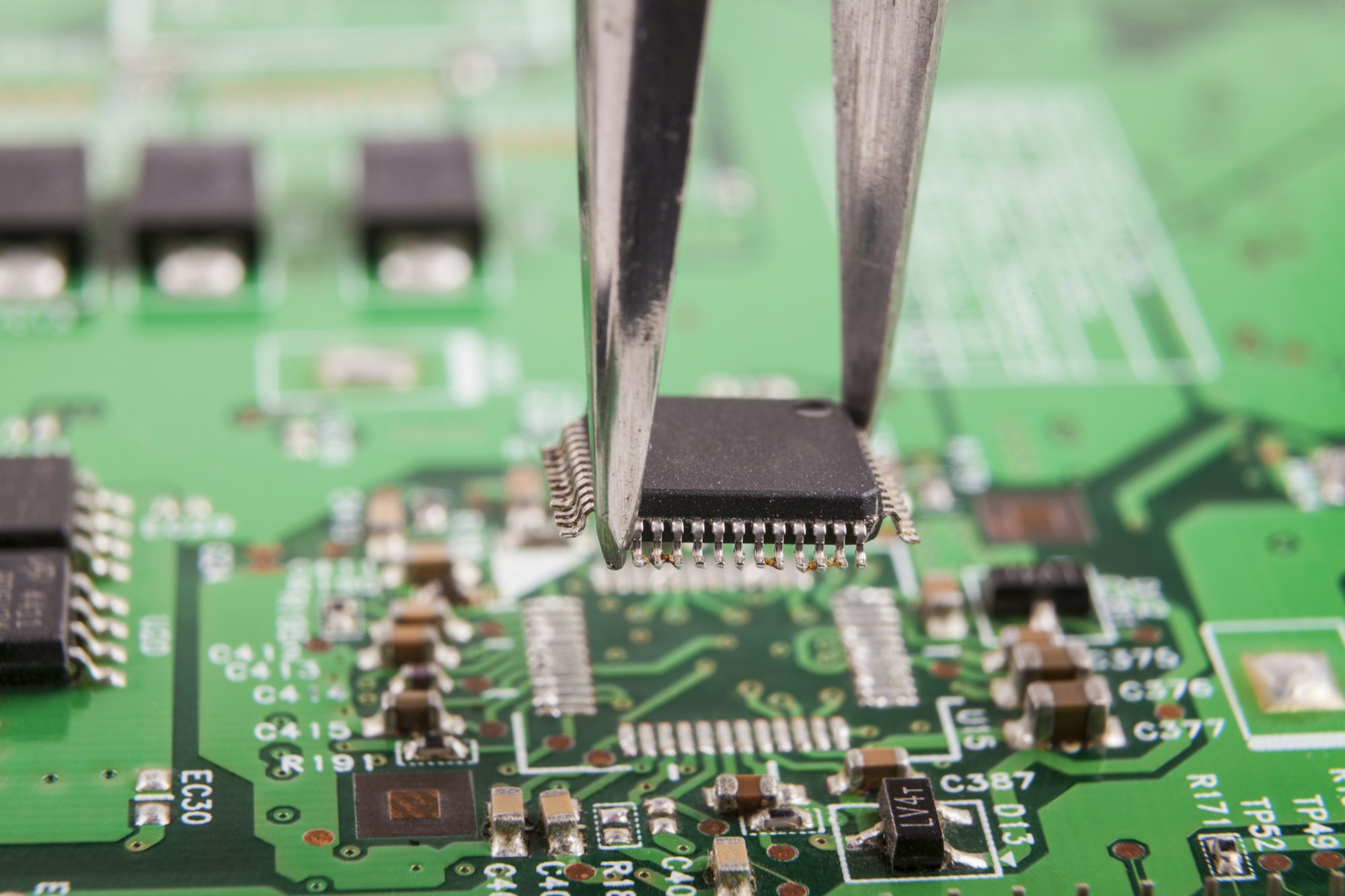
Struggling with PCB design? Feeling overwhelmed by options? You're not alone. The right tool changes everything.
Choosing a PCB design1 platform depends on your specific needs, budget, and project complexity. For many, a web-based, collaborative tool like EasyEDA2 offers a strong, accessible solution.
I've spent countless hours navigating the world of PCB design, and I know firsthand how critical it is to pick the right platform. Let's dive into what makes a platform stand out.
How to Optimize PCB Design?
Is your PCB design process slowing you down? Are errors costing you time and money? There is a better way.
Optimizing PCB design involves streamlining your workflow, utilizing effective software features, and focusing on best practices. This ensures efficiency, reduces mistakes, and improves overall project success.

When I optimize my PCB designs, I look at several key areas. These strategies help me reduce iterations and get to a working prototype faster.
Understanding Your Workflow
First, you need to understand your current process. Where are the bottlenecks? What tasks take the most time?
| Step | Description | Improvement Focus |
|---|---|---|
| Schematic Capture | Laying out electrical connections. | Component library accuracy, symbol creation. |
| Component Selection | Choosing parts for the design. | Availability, cost, footprint. |
| PCB Layout | Arranging components and traces on the board. | Routing efficiency, DRC checks. |
| Verification | Checking for errors and design rule violations. | Automated DRC, simulation. |
Leveraging Software Features
Modern PCB tools offer powerful features. Using them effectively is key. I find that features like hierarchical design, design rule checking (DRC)3, and integrated simulation save me a lot of time. For example, EasyEDA's real-time collaboration lets my team work together seamlessly, avoiding version control headaches.
Best Practices for Efficiency
I also follow specific best practices. This includes creating reusable design blocks, maintaining organized component libraries, and performing regular design reviews. These steps ensure my designs are not only functional but also easy to maintain and scale.
How to Ensure Design for Manufacturability (DFM) in PCB Design?
Are you tired of manufacturing delays and costly board revisions? Do your designs often come back with production issues? DFM is your answer.
Ensuring Design for Manufacturability (DFM)4 means designing your PCB to be easily and cost-effectively produced. This involves considering manufacturing constraints early in the design process to prevent issues.

My experience tells me that ignoring DFM costs you more in the long run. I always focus on these aspects to make sure my boards come out right the first time.
Why DFM is Critical
DFM isn't just about avoiding errors; it's about saving money and time. If a board is hard to manufacture, it leads to higher production costs, longer lead times, and potential quality issues. I learned this the hard way on a project where a seemingly minor trace width5 caused major headaches on the assembly line.
Key DFM Considerations
I always keep several DFM aspects in mind during design.
| DFM Aspect | Description | Design Guideline |
|---|---|---|
| Trace Width/Spacing | Minimum distances between traces and pads. | Adhere to manufacturer's capabilities. |
| Pad Size/Shape | Size and shape of component pads. | Ensure proper solder joint formation. |
| Via Size/Type | Diameter and type of vias (through-hole, blind). | Use standard sizes to reduce cost. |
| Component Placement | How components are arranged on the board. | Ensure accessibility for assembly and rework. |
| Solder Mask Relief | Opening in the solder mask around pads. | Proper clearance prevents solder bridging. |
DFM Tools and Checks
Many modern PCB design platforms, like EasyEDA, include built-in DFM checks. I use these tools religiously to catch potential issues before sending files to the manufacturer. This proactive approach has saved me from countless production delays and rework costs. It is always better to fix an issue on screen than on a finished board.
Are You Ready for High-Speed, Flexible, and HDI PCB Design?
Are your current designs pushing the limits of standard PCBs? Do you need more performance, smaller form factors, or dynamic flexibility? It's time to adapt.
High-speed, flexible, and High-Density Interconnect (HDI) PCB designs demand specialized knowledge and tools. They offer advanced capabilities but require careful planning and precise execution.

I remember a project where standard PCBs just wouldn't cut it. That's when I realized the importance of mastering these advanced PCB design techniques.
High-Speed Design Essentials
When I tackle high-speed designs, signal integrity is my top priority. This means managing impedance, reducing crosstalk, and ensuring proper termination. For example, differential pairs need careful routing to maintain signal quality.
| High-Speed Factor | Importance | Design Implication |
|---|---|---|
| Impedance Control | Prevents signal reflections. | Trace width, dielectric constant, layer stack-up. |
| Crosstalk | Undesired coupling between adjacent traces. | Spacing, ground planes. |
| Termination | Matching trace impedance to load impedance. | Resistors at ends of traces. |
| Layer Stack-up | Arrangement of conductive and insulating layers. | Ground and power planes for shielding. |
Flexible PCB Design Challenges
Flexible PCBs introduce a whole new set of considerations. Bending and flexing affect material choices, trace routing, and component attachment. I often use thinner copper and specific flexible substrates. For example, a common pitfall is placing components in areas that will experience extreme bending.
HDI PCB Advantages
HDI designs allow for higher component density and smaller form factors. This is achieved through microvias, finer lines, and advanced stacking technologies. I've used HDI to shrink board size significantly, which was crucial for a compact wearable device I designed. It’s a powerful technique when space is at a premium.
Conclusion
Choosing a PCB design platform is a personal journey. EasyEDA provides a fantastic starting point for many, offering powerful, accessible features for a wide range of projects.
Explore this link to discover essential practices that can enhance your PCB design process and efficiency. ↩
Learn about EasyEDA's unique features that make it a top choice for PCB design, especially for collaborative projects. ↩
Discover how DRC can help you catch errors early in the PCB design process. ↩
Understand the importance of DFM in PCB design to avoid costly manufacturing issues. ↩
Learn how trace width impacts signal integrity and manufacturing in PCB design. ↩


