
You spent weeks designing your PCB layout. Now blurry text ruins your assembly. Wrong orientations delay production. Poor markings add hours of troubleshooting. You need the right identification solution to prevent costly errors.
Direct Legend Printing (DLP)[^1] delivers superior detail for complex designs, while Liquid Photo Imaging (LPI) balances precision and cost efficiency. Traditional screen printing[^2] offers budget options for low-detail boards. The "best" method depends entirely on your design complexity, tolerance needs, and budget constraints – no universal solution exists.
Choosing silkscreen technology[^3] impacts your PCB’s assembly success. Read on to understand how each method solves specific problems. We’ll explore functionality, manufacturing details, and failure points to guide your decision.
What does silkscreen do?
Your PCB looks bare without identifiers. Workers use silkscreen daily during assembly and testing. Mislabeled components lead to disastrous mistakes where a single resistor swap scraps a batch.
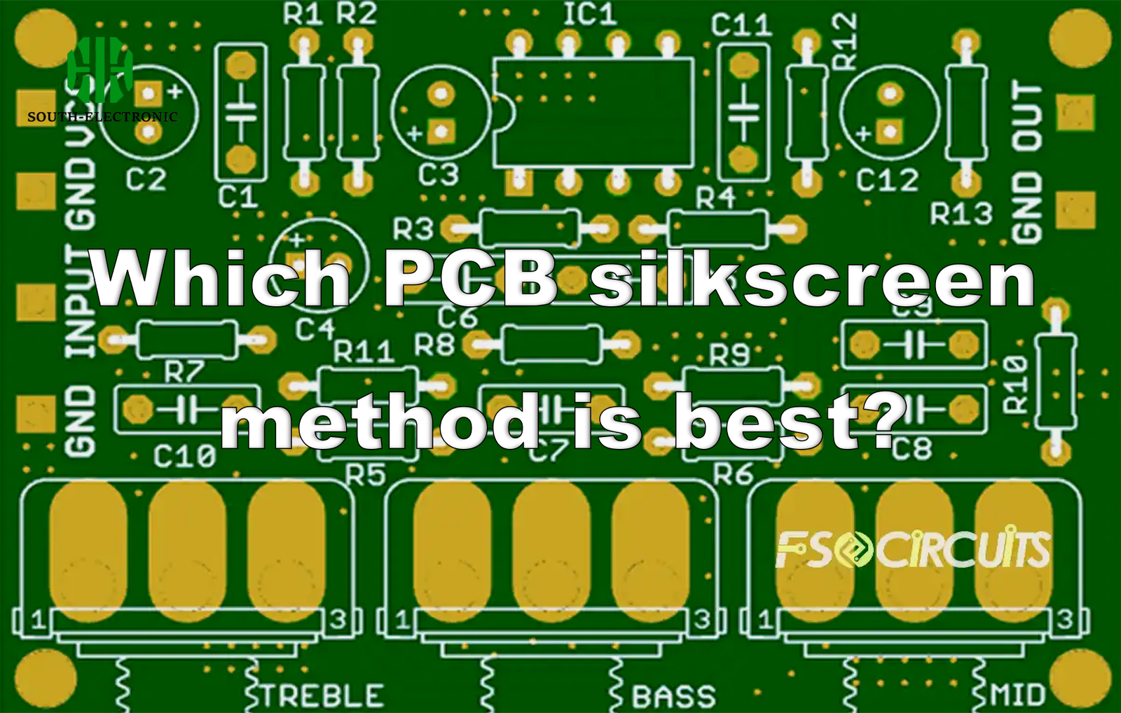
Silkscreen marks component positions, orientations, testing points, and brand information on PCBs. These markings help technicians place parts accurately, troubleshoot failures safely, and prevent dangerous assembly errors. This functional layer serves as permanent assembly instructions.
Core functions and applications
Silkscreen serves three primary purposes across production lifecycles. This table breaks down crucial use cases:
| Function Type | Implementation Examples | Prevented Errors |
|---|---|---|
| Component ID | R9, C12, D3 markers | Wrong part placement |
| Polarization | Diode/reference marks | Reversed components |
| Safety & Info | High-voltage warnings | Test point confusion |
During prototyping last month, I fixed a layout where absent inductor polarity markings caused 40% boards failures. Silkscreen must withstand soldering heat since rework happens commonly. Newer PCBs require finer lines for micro-component marks. Technicians need visible warnings near hazardous circuits as small as 0402 components. Markings also assist debugging processes after months of field use by reducing troubleshooting time significantly.
How thick is PCB silkscreen?
Inconsistent ink thickness causes problems when you use thin stencils. Your solder paste application gets uneven. Text smears easily across pads during handling. Poor thickness control blocks microscopic components.
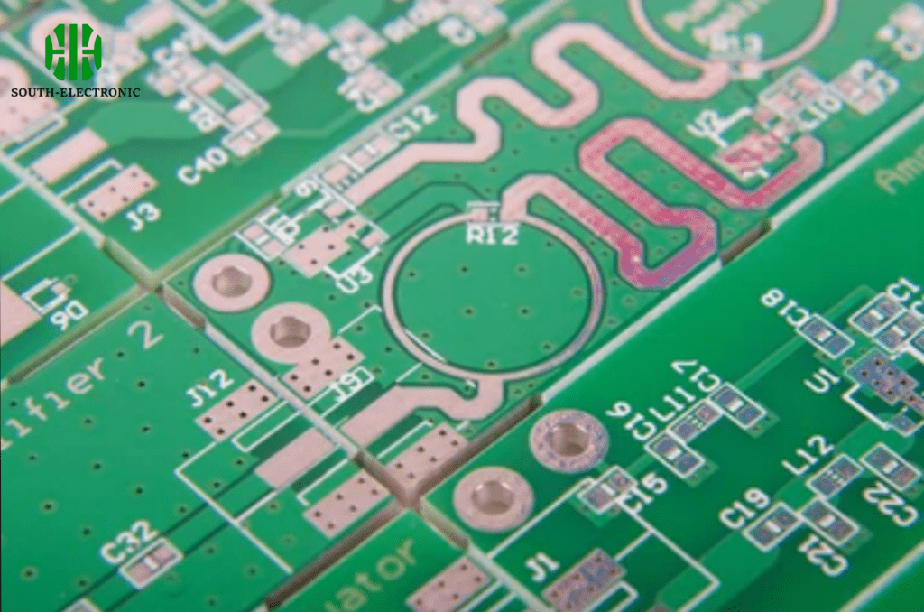
Standard silkscreen measures 0.1–0.15mm thick but varies by application method. DLP creates ultra-thin 25–50μm layers. LPI coatings hit 45–75μm. Traditional screening forms thickest markings at 50–150μm. Lower thickness improves finer detail with tighter clearance requirements.

Tolerance effects and methodology comparison
Thickness variations impact PCB performance differently across fabrication methods. These critical technical factors determine successful application:
| Method | Thickness Range | Detail Limit | Edge Clearance Risk |
|---|---|---|---|
| Screen Printing | 50–150 microns | 0.15mm | High (>0.2mm gap needed) |
| LPI | 45–75 microns | 0.10mm | Medium (>0.15mm gap) |
| DLP | 25–50 microns | 0.05mm | Low (>0.08mm gap) |
Thicker silk reduces placement accuracy substantially in dense designs. For instance, a 150μm layer could bridge onto pads. Last summer I saw a board where thermal cycling cracked screen-print ink from thickness changes. DLP avoids this with its hardened process. High-density BGAs get assembly errors over 100μm due to obscuring pads. Environmental factors also affect layer integrity differently for each method.
What are common silkscreen nightmares?
Your manufacturer sends boards with blurry numbers. Your client rejects units with smudged logos. Assembly halts because rotated markings cause capacitor explosions. These recurring failures cost money and time repeatedly.
Common nightmares include blurred/distorted markings, ink bleed onto pads, incorrect alignments obscuring pins, poor adhesion causing flaking, and color mismatch. These defects cause assembly errors, test failures, premature wear, and non-compliance rejections during inspections.
Failure modes and prevention solutions
Critical defects emerge from specific process failures that each method counters differently. Use this breakdown to avoid production disasters:
| Failure Mode | Primary Cause | Best Prevention Method |
|---|---|---|
| Blurry Text | Stencil distortion | DLP (direct laser etching) |
| Pad Contamination | Ink bleeding | LPI (photo development precision) |
| Adhesion Failure | Surface prep failure | Plasma treatment pre-coating |
| Registration Drift | Alignment error | Optical positioning systems |
I once scrapped 300 boards when screen-printed logos flaked off vibration testing. DLP eliminates adhesion problems chemically by etching solder mask. Registration errors below 0.1mm offset plague manual setups. Environmental compliance matters too – I’ve seen military contracts voided when labels lacked RoHS markings near lead. Prevention saves repair expenses exceeding fabrication costs multiple times over.
Conclusion
DLP excels for precision needs, LPI suits most applications well, and screen printing works for simple, low-cost PCBs. Always match the silkscreen method to your specific project needs.
[^1]: Explore how DLP enhances detail and precision in PCB designs, ensuring high-quality assembly.
[^2]: Discover the budget-friendly options of traditional screen printing for low-detail PCB projects.
[^3]: Understand the impact of silkscreen technology on PCB assembly success and error prevention.

