
You’re squinting at project budgets. Costs keep climbing. Why does this happen with ceramic PCBs? Understanding the price difference helps you make smarter decisions for your electronics.
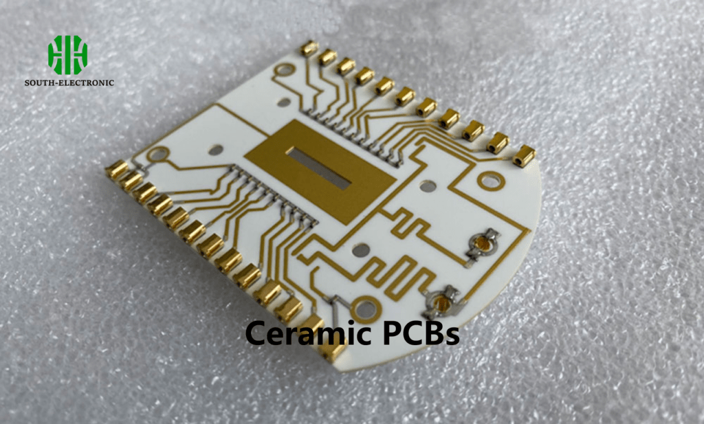
Ceramic PCBs cost more than FR4 boards due to pricier materials like aluminum nitride and complex manufacturing. Processes such as high-temperature sintering require specialized equipment. This increases production expenses but delivers superior thermal performance for demanding applications.
Now let’s examine specific scenarios where this investment matters most. Comparing material options reveals true value trade-offs.
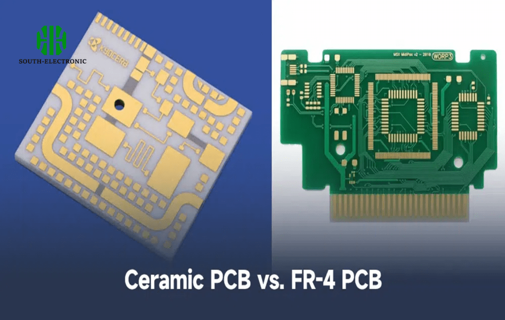
Ceramic vs. FR4 Multilayer PCBs: When Does Your Project Demand the Switch?
Your board warps under heat stress. Circuit failures frustrate you. Identify critical thresholds to justify ceramic adoption.
Switch to ceramic PCBs[^1] when operating above 150°C or needing under 0.5% signal loss. High-power RF modules like radar systems require ceramic’s stability. Automotive sensors in engines need zero thermal deformation.
Key Comparison Factors
Consider these distinctions before changing materials:
| Property | Ceramic PCBs | FR4 PCBs | Impact |
|---|---|---|---|
| Max Temperature | 350°C+ | 130°C-150°C | High-power device reliability |
| Thermal Conductivity | 24-180 W/mK | 0.3 W/mK | Heat dissipation efficiency |
| Dielectric Loss | 0.0003 | 0.02 | Signal integrity in GHz ranges |
| Production Cost | 5-8× higher | Baseline | Project budget allocation |
I once redid an aerospace project after FR4 boards cracked during thermal cycling tests. Ceramic versions handled extreme temperature swings perfectly. This experience taught me to calculate total lifecycle costs. Material expenses matter less than system failures in mission-critical applications. Multilayer designs amplify these differences since ceramic layers bond better at high temperatures with near-zero thermal expansion mismatches. Always evaluate operating temperatures first.
How to design reliable thermal management for ceramic PCBs?
Hotspots trigger early failures. You need predictable performance. Optimize heat pathways to prevent this.
Place copper-plated thermal vias beneath heat sources like ICs. Use aluminum nitride substrates for critical components. Prioritize direct thermal connections to metal cores or heat sinks.
Thermal Design Framework
Manage temperatures systematically:
| Layer | Function | Material Tip |
|---|---|---|
| Core Substrate | Primary heat pathway | AlN (170-180 W/mK conductivity) |
| Circuit Traces | Spread heat laterally | Thick-copper (>200µm) deposition |
| Interface Material | Connect components to board | Silver-filled epoxy adhesives |
| External Cooling | Dissipate heat from assembly | Integrated copper heat spreaders |
I learned thermal management[^2] principles the hard way when a prototype LED array failed. Without thermal vias, heat concentrated under drivers. We redesigned with conductive alumina ceramic pcb patterns. Temperature dropped 40°C. Now I model hotspots early. Good thermal management reduces operating stress. It extends product lifespan significantly.
How to solve 5 common ceramic PCB production issues[^3]?
Cracks during manufacturing delay delivery. Defects frustrate your team. Apply targeted solutions for smoother production.
Tackle warping with controlled kiln cooling rates. Prevent metallization peeling using surface laser activation. Solve micro-cracks through optimized sintering profiles.
Production Challenges and Fixes
Common issues and corrective actions:
| Issue | Cause | Solution |
|---|---|---|
| Substrate Warping | Rapid cooling phase | Gradual temperature ramping |
| Trace Delamination | Poor ceramic/metal bonding | Surface roughening pre-treatment |
| Via Cracking | CTE mismatch | Ductile gold plating in holes |
| Drilling Fractures | Brittle ceramic material | Laser micromachining technique |
| Solder Leakage | Uneven surface porosity | Double-layer metallization |
I visited a ceramic pcb manufacturer struggling with 20% wastage rates. Adjusting press pressure solved substrate inconsistencies. Production yields jumped after implementing statistical process controls. Getting prototypes made helps tweak variables. Solving these problems requires experienced ceramic pcb suppliers who monitor every manufacturing stage closely.
Conclusion
Ceramic PCBs cost more due to materials and precision manufacturing. Choose them for extreme environments where thermal stability prevents system failure.
[^1]: Explore the benefits of ceramic PCBs to understand their value in high-performance applications, ensuring your projects meet demanding requirements.
[^2]: Learn effective strategies for thermal management to enhance reliability and performance in your electronic projects, preventing costly failures.
[^3]: Discover solutions to common ceramic PCB production challenges to improve efficiency and reduce waste in your manufacturing process.


