

I once fried a prototype board where insulation failed. That painful moment made me realize how crucial non-conductive materials truly are for preventing disaster in electronics. Let’s uncover their invisible lifesaving role.
Non-conductive layers provide essential electrical insulation between copper traces, support mounting components, and manage heat dissipation in PCBs. Their precise dielectric properties prevent short circuits while enabling signal integrity – forming the silent foundation all circuitry depends on.
Understanding this insulation need leads us logically to material selection considerations. Design choices dramatically impact board reliability under thermal, mechanical, and electrical stress during use.
How do you choose the right non-conductive material for your PCB?
Your circuit board faces unique environmental challenges. Material mismatch could trigger failures when temperatures fluctuate or vibrations strike unexpectedly. This critical decision demands careful assessment.
Prioritize operating environment factors including temperature range, frequency needs, regulatory compliance, and cost-effectiveness first. Then contrast materials’ relative permittivity, thermal conductivity, and mechanical strength using standardized qualification testing methods.
Evaluation criteria breakdown
Selecting insulation involves balancing four core performance parameters against your project needs. Consider their interplay rather than isolated specs.
Dielectric reliability
High-frequency designs need stable dielectric constants to maintain signal timing accuracy. Low-loss tangents preserve voltage levels instead of wasting energy as heat.
Heat handling capacity
Thermal management directly links to system lifespan. Glass Transition Temperature (Tg) denotes structural integrity limits – exceeding this warps boards. Heat dissipation ability affects component cooling.
| Parameter | FR-4 Standard | High-Frequency Alternative | High-Thermal Alternative |
|---|---|---|---|
| Dielectric Constant | 4.3-4.9 | 3.2-3.6 | 4.0-4.5 |
| Loss Tangent | 0.02 | 0.001 | 0.012 |
| Max Operating Temp | 130°C | 150°C | 170°C |
| Thermal Conductivity | 0.3 W/mK | 0.5 W/mK | 1.5 W/mK |
Mechanical stability
Flex boards require elastic modulus compliance. Rigid applications demand resistance to expansion from thermal cycling. Impact resistance prevents damage during handling.
Certification compliance
Flammability ratings like UL94 V-0 remain vital for safety approvals. REACH/RoHS compliance avoids toxic substances in manufacturing. Industrial standards govern material validation procedures.
Testing prototypes under simulated environmental conditions validates choices better than theoretical specs. I always build three material sample groups – this extra step caught thermal expansion issues early during one medical device project.
What are the essential non-conductive materials used in PCB manufacturing?
Ever wondered what protects conductive patterns once laminated? Industry-standard choices include fiberglass-reinforced epoxy alongside novel polymer options. Each solves specific performance challenges uniquely.
Common dielectric materials are FR-4 epoxy resin, polyimide film, polytetrafluoroethylene, and ceramic-filled hydrocarbon polymers. These provide differing combinations of thermal resistance, mechanical flexibility and signal loss characteristics for specific applications.

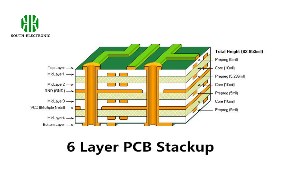
Core vs Prepreg differences
The sandwich structure uses two distinct material formats to create layered insulation and bonding:
Base/core dielectric
Constitutes the rigid structural foundation of circuit board. Pre-impregnated fiberglass (FR-4) remains the standard for conventional electronics. Alternatives include thermal-conductive ceramics or bendable polyamides.
Prepreg bonding sheets
Act as adhesive layers between laminated copper and cores when heated. Their partially cured resin flows before hardening to fill gaps completely. Prepreg resin content determines final dielectric thickness.
| Material Type | Key Properties | Common Applications | Limitations |
|---|---|---|---|
| FR-4 | Low cost, balanced performance | Consumer electronics | Limited thermal performance |
| Polyimide | Extreme temperature endurance | Aerospace, automotive, flex | Higher cost |
| PTFE/Teflon | Lowest signal loss at high GHz | RF/5G equipment | Difficult machining |
| Ceramic | Superior thermal conductivity | Power modules, LED lighting | Brittle, heavy |
Each material undergoes extensive preprocessing: reinforcing fibers get woven into fabrics then impregnated with resin systems. Manufacturers create custom formulations matching dielectric values to impedance targets. Material science innovation continues evolving these composites – I recently tested an experimental nanoclay-infused resin that doubled thermal endurance versus traditional FR-4.
Can you plate non-conductive materials for PCBs?
Many believe holes in dielectric substrates require conductive connections. The secret answer: specialized plating techniques transform insulators into conductive pathways for drilling.
Printed circuit boards achieve conductivity on non-conductive materials using electroless copper deposition before electroplating. The seeding process chemically deposits conductive metal particles onto dielectric surfaces and through-hole walls.

Critical manufacturing process phases
Building reliable plated connections demands careful execution at three vital stages:
Cleaning and conditioning
First, alkaline cleaners remove organic contaminants. Then chemical etching roughens surfaces on non-conductive materials. Microscopic anchors help subsequent layers lock mechanistically onto non-conductive materials.
Activation catalyst seeding
Palladium-based solutions deposit metallic nuclei across treated surfaces. These catalytic sites initiate electron exchange reactions during subsequent copper deposition. Uniform coating ensures void-free coverage later.
Metal deposition development
Electroless copper then chemically grows around particles to form conductive base layers. Next, electroplating thickens metallization for handling assembly stress through barrel-filled holes.
Failure causes like pinholes or peel-off usually originate at cleaning defects. Manufacturers track surface tension values using dyne testing pens before seeding. For high-density interconnects, I’ve seen labs use plasma etching instead of wet chemicals to achieve finer hole walls at microscopic levels – enabling advanced packaging requirements. Thermal stresses during plating remain tightly controlled to prevent interfacial cracks developing under component solder joints after production.
Conclusion
Non-conductive materials truly form the functional core of modern electronics. Their selection and processing ultimately determines circuit board performance in critical isolation roles across every device we use daily.

