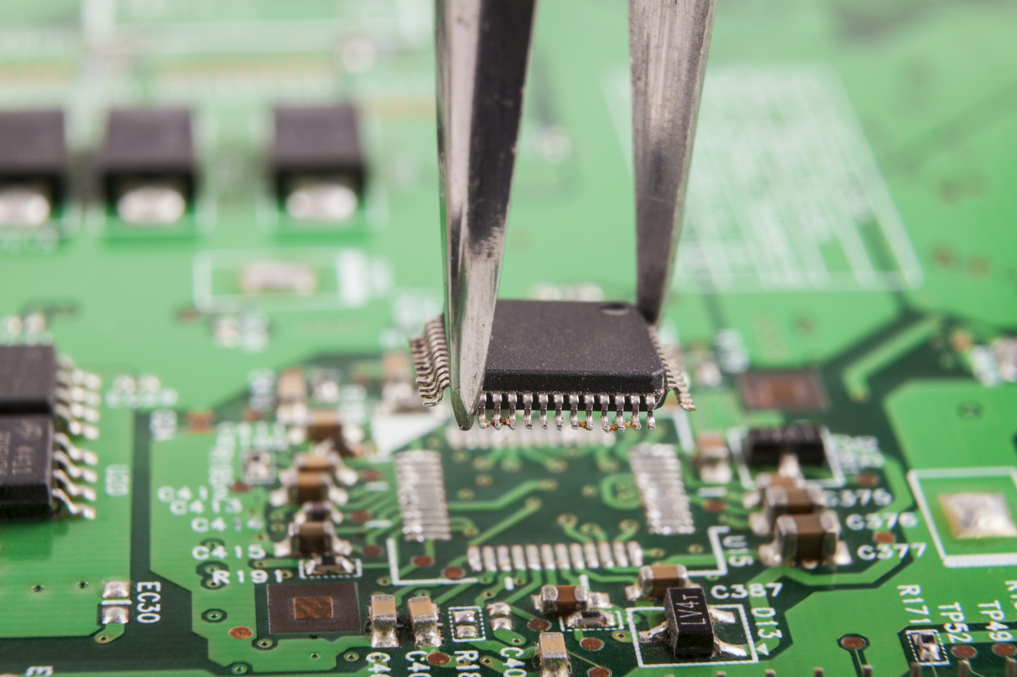
Your resistor suddenly smells like burnt plastic? Smoke curls from your circuit board? Overheating resistors kill projects and waste hours. Let’s fix this frustrating problem together.
PCB resistors overheat when they exceed power ratings, suffer poor thermal design, or face high ambient heat. To prevent it, calculate load currents accurately, ensure proper airflow, and select components rated for at least 2× your expected power.
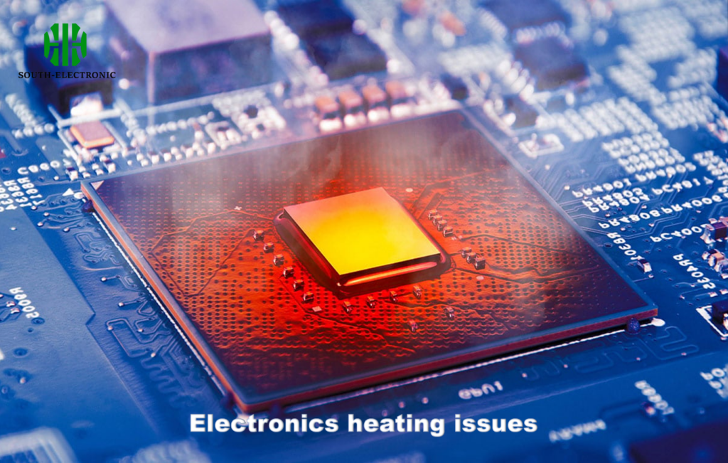
Now that we know the basics, I’ll show you practical steps to diagnose and resolve these overheating issues.
How to Identify and Troubleshoot Resistors on Circuit Boards?
Is that brown spot on your PCB a failing resistor? Overlooked signs can lead to catastrophic board failure. Catch issues early with these methods.
Start with a visual inspection for discoloration or cracking. Next, use a multimeter in circuit to measure resistance shifts from labeled values. Finally, verify voltage drops during operation using thermal cameras.
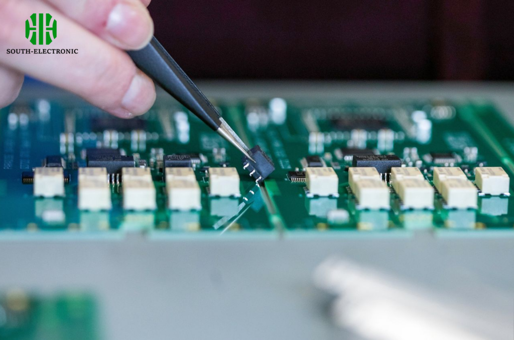
Step-by-Step Diagnostic Approach
I once spent days debugging a ghost issue before realizing a tiny 0603 resistor was overheating at peak loads. Follow this workflow:
-
Power-off inspection:
Check for:- Charring around solder joints
- Swollen component bodies
- PCB discoloration
-
Resistance validation: Measurement Normal Result Fault Indicator In-circuit ±10% of value 50%+ deviation Desoldered Exact rating Open/infinite ohms
Power up and measure voltage drop across the resistor (V = I×R).
Exceeding power ratings (P = I²×R) confirms overload. Finally, confirm with thermal imaging – hotspots >100°C demand action.
Embedded Resistors in PCBs: Are They Worth the Cost for High-Speed Designs?
Struggling with signal reflections at 5GHz+? Traditional resistors introduce parasitic capacitance that ruins high-speed signals. Embedded alternatives offer solutions – but at a price.
Integrated thin-film resistors directly in PCB layers reduce parasitics by 30-40%. They cost 20% more upfront but minimize impedance mismatches critical for RF/memory designs, making them viable for high-frequency projects.
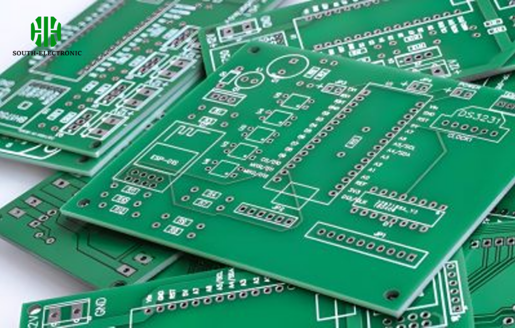
When to Choose Embedded Resistors
I reserve embedded tech for clients needing >3 GHz signal integrity. Key factors:
Pros for High-Speed:
- Reduced EMI from shorter current loops
- Eliminated component tombstoning risk
- Consistent impedance across batches
Cons For Budgets:
- Zero post-assembly value adjustments
- 48-hour turnaround for design changes
- Limited resistance range
| Scenario | Conventional Better? | Embedded Better? |
|---|---|---|
| Prototyping | ✓ | ✗ |
| >4 Layer HDI | ✗ | ✓ |
| Cost-sensitive | ✓ | ✗ |
| RF/Server Boards | ✗ | ✓ |
Through-Hole vs SMD Resistors: Which Wins for Prototyping and Repair?
Snapping leads while swapping components? Through-hole provides hand-solder ease but wastes space. New designers face this tradeoff daily.
Through-hole wins for prototyping with breadboards and manual rework. SMD suits production runs. Keep both: use 1206 SMD for easy hand-soldering repairs, and reserve through-hole for high-power test points.

Real-World Repair Scenarios
Last month, I fixed an industrial controller where SMD resistors cracked from vibration. The solution? Hybrid approach:
Through-Hole Advantages:
- Easier visual inspection
- Withstands mechanical stress
- Simplifies circuit modifications
SMD Advantages:
- 70% smaller footprint
- Lower parasitic inductance
- Faster automated assembly
| Task | Recommended Type | Why |
|---|---|---|
| Breadboarding | Through-hole | Push-fit compatibility |
| Rework under microscope | 0805+ SMD | Precise soldering |
| High-vibration | Through-hole | Stronger anchors |
| >500 MHz circuits | SMD | Shorter paths |
Resistor Footprint Design: Best Practices for Avoiding Assembly Defects
90% of soldering defects trace back to footprint errors. Tombstoned resistors and cold joints cost thousands in rework. Prevent them upfront.
Always match pad sizes to component terminals with 0.1mm tolerance. Implement thermal relief gaps on power traces. Orient all resistors parallel to reflow oven direction to prevent uneven heating.
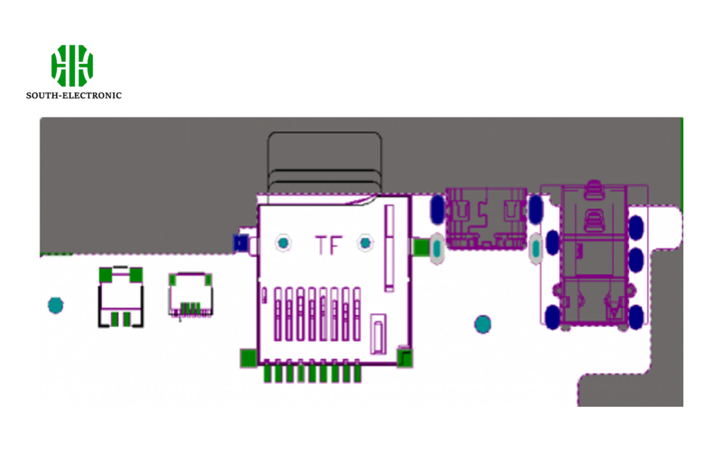
Critical Dimensions and Patterns
I standardized these footprint rules after a batch failure cost $3k in scrap:
Pad Geometry Rules:
- SMD pad length = component length + 0.3mm
- Pad spacing = exact resistor terminal spacing
- Thermal relief width = 50% of trace width
Common Defect Solutions:
| Issue | Cause | Fix |
|---|---|---|
| Tombstoning | Uneven pad heating | Symmetric pad sizing |
| Solder balls | Excess paste | Reduce stencil to 90% pad area |
| Cracked joints | Rigid connections | Add 0.1mm solder mask between pad and plane |
Conclusion
Prevent resistor overheating through accurate power calculations, thermal design, and smart component choices. Test early and design footprints carefully.


