
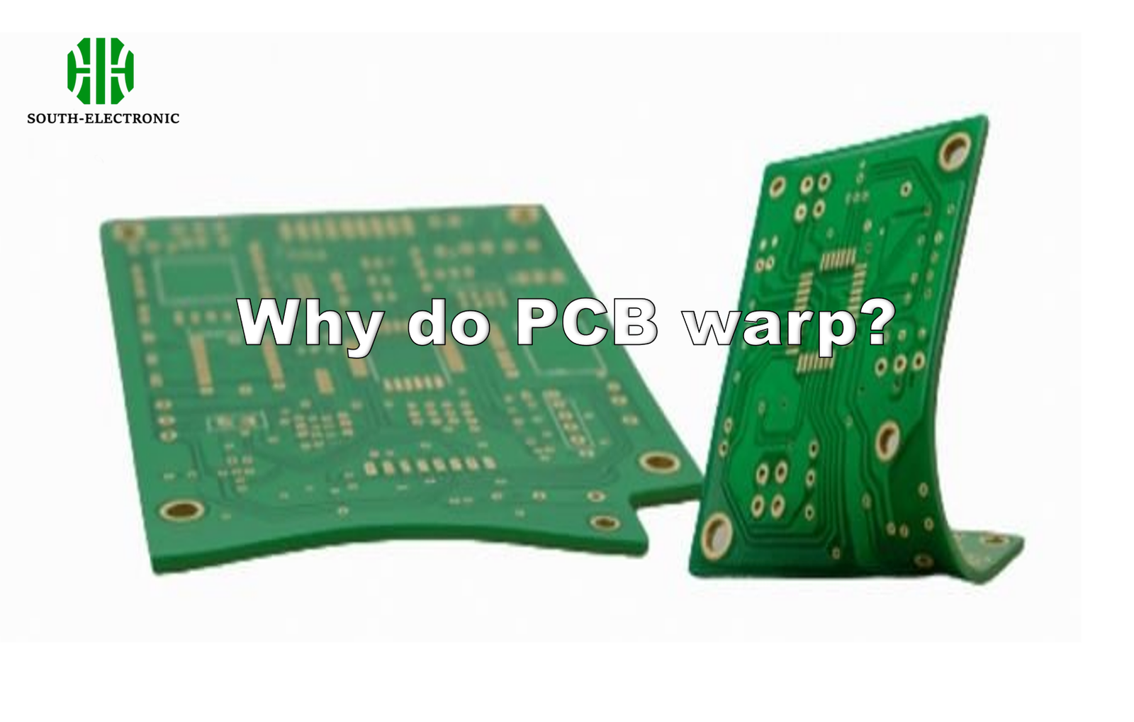
What are the dangers of PCB warping?
-
On automated surface mount assembly lines, uneven circuit boards can cause inaccurate positioning, making it difficult to insert or place components into holes and surface mount pads on the board. It can even damage the automated assembly machine.
-
After soldering, a circuit board with components on it can bend, making it difficult to trim component leads evenly. The board can also be difficult to install into a computer chassis or sockets within the machine. Therefore, encountering warped boards is also a significant problem for assembly plants.
Current surface mount technology is developing towards high precision, high speed, and intelligent technology. This places even higher demands on the flatness of PCBs, the home of various components.
The IPC standard specifically states that the allowable deformation of PCBs with surface mount devices is 0.75%, while the allowable deformation of PCBs without surface mount devices is 1.5%.
In fact, to meet the demands of high-precision and high-speed placement, some electronics assembly manufacturers have even stricter requirements for deformation tolerance, such as a 0.5% allowable deformation, and some even require 0.3%.
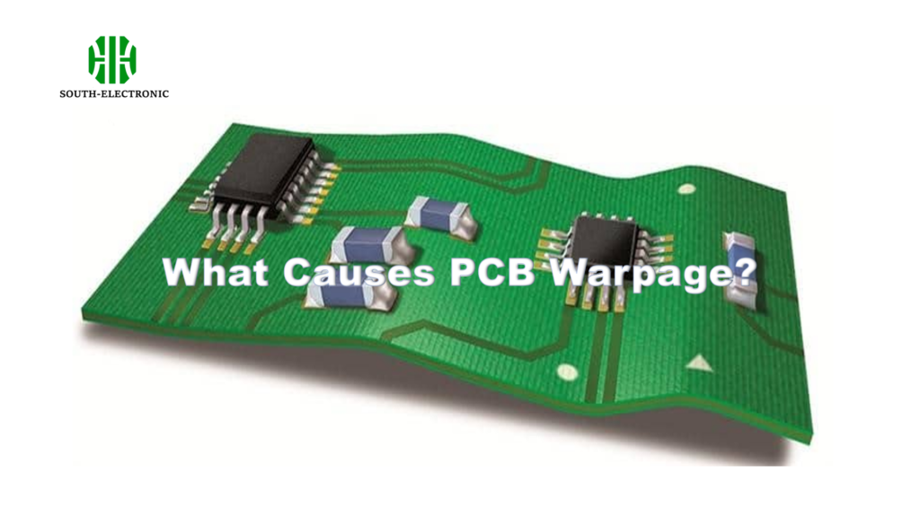
PCBs are composed of materials such as copper foil, resin, and glass cloth. Each material has different physical and chemical properties. Pressing them together inevitably generates residual thermal stress, leading to deformation.
In addition, during the PCB manufacturing process, various processes such as high temperatures, mechanical cutting, and wet processing can also significantly affect board deformation. In short, the causes of PCB deformation are complex and diverse. Reducing or eliminating deformation caused by varying material properties or processing has become a complex issue facing PCB manufacturers.
Analysis of Causes of PCB Deformation
PCB deformation requires investigation from several perspectives, including material, structure, pattern distribution, and processing steps. This article will analyze and explain the various possible causes of deformation and how to mitigate them.
-
Uneven copper surface area on the PCB can exacerbate board bowing and warping.
-
PCBs typically feature large areas of copper foil for grounding, and sometimes the Vcc layer also features large areas of copper foil. When these areas are not evenly distributed across the board, uneven heat absorption and heat dissipation can occur.
-
PCBs naturally expand and contract with heat. If these expansions and contractions are not synchronized, they will cause differential stresses and deformation. If the board’s temperature reaches its upper limit of Tg, the board will begin to soften, causing deformation.
-
The connections between layers on the PCB (vias) limit board expansion and contraction.
-
Most current PCBs are multilayer, and layers have rivet-like connections (vias). These connections are categorized as through-holes, blind vias, and buried vias. These connections limit board expansion and contraction, indirectly causing board bowing and warping.

Causes of PCB Deformation:
- The weight of the PCB itself can cause it to sag and deform.
Typically, reflow ovens use chains to propel the PCB forward, using the sides of the PCB as support points.
If the PCB is loaded with heavy components or is too large, its weight can cause it to sag in the middle, causing the PCB to bend.
- The depth of the V-cut and the connecting strips can affect the amount of deformation in the assembled PCB.
V-cuts are essentially the culprit for damaging the PCB structure. Because they create grooves in a larger sheet of PCB material, they are prone to deformation.
- The impact of lamination materials, structure, and pattern on PCB deformation:
PCBs are made by laminating a core board, a prepreg sheet, and an outer layer of copper foil. The core board and copper foil deform under heat during lamination, and the amount of deformation depends on the coefficient of thermal expansion (CTE) of the two materials.
The coefficient of thermal expansion (CTE) of copper foil is approximately 17 x 10-6. The Z-direction CTE of ordinary FR-4 substrate below its Tg point is 50-70 x 10-6, and above its Tg point, it is 250-350 x 10-6. Due to the presence of glass cloth, the X-direction CTE is generally similar to that of copper foil.
How to Prevent PCB Warping
Warping has a significant impact on printed circuit board (PCB) production and is a key issue in the PCB manufacturing process. Boards with components mounted on them can bend after soldering, making it difficult to align component leads. The board can also be difficult to install in a computer chassis or sockets within the device. Therefore, PCB warping can affect the proper functioning of all subsequent processes.
- Considerations for PCB Design:
A. The prepreg sheets between layers should be arranged symmetrically. For example, in a six-layer board, the thickness and number of prepreg sheets between layers 1-2 and 5-6 should be consistent. Otherwise, warping is likely to occur after lamination.
B. The core board and prepreg for a multilayer board should be from the same supplier.
C. The circuit pattern areas on the outer layers, Sides A and B, should be as close as possible. If Side A has a large copper surface and Side B has only a few traces, the printed circuit board will easily warp after etching. If the circuit area difference between the two sides is too great, some independent grids can be added to the sparser side to balance it out.
-
Baking the board before cutting:
Baking the copper-clad laminate before cutting (150°C for 8 ± 2 hours) aims to remove moisture from the board and fully cure the resin within the board, further eliminating any residual stress, which helps prevent warping. -
Warp and Weft Directions of the Prepreg:
After lamination, the shrinkage rates of the prepreg in the warp and weft directions differ. Therefore, the warp and weft directions must be carefully distinguished during cutting and stacking. Otherwise, warping of the finished board after lamination is likely to occur, which is difficult to correct even with pressure baking. -
Post-Lamination Stress Relief:
After hot and cold pressing, remove the multilayer board, trim or mill off any burrs, and then place it flat in an oven at 150°C for 4 hours to gradually release stress and fully cure the resin. This step is essential. -
Straightening Thin Boards During Electroplating:
Special clamping rollers are required for surface and pattern plating of ultra-thin multilayer boards (0.4-0.6mm). After clamping the thin boards onto the flybar on the automated plating line, a round rod is used to connect the clamping rollers along the entire flybar, thereby straightening all the boards on the rollers and preventing deformation after electroplating. -
Dealing with Warped Boards:
In well-managed factories, printed boards undergo a 100% flatness inspection during final inspection. Unqualified boards are removed and placed in an oven, where they are baked at 150°C under heavy pressure for 3-6 hours and then allowed to cool naturally under heavy pressure.
Then, the pressure is released and the board is removed for a flatness check. This can save some boards, but some boards may need two or three rounds of baking and pressing to level them. If the above-mentioned anti-warping process measures are not implemented, some boards will be useless even after baking and pressing and will have to be scrapped.

