
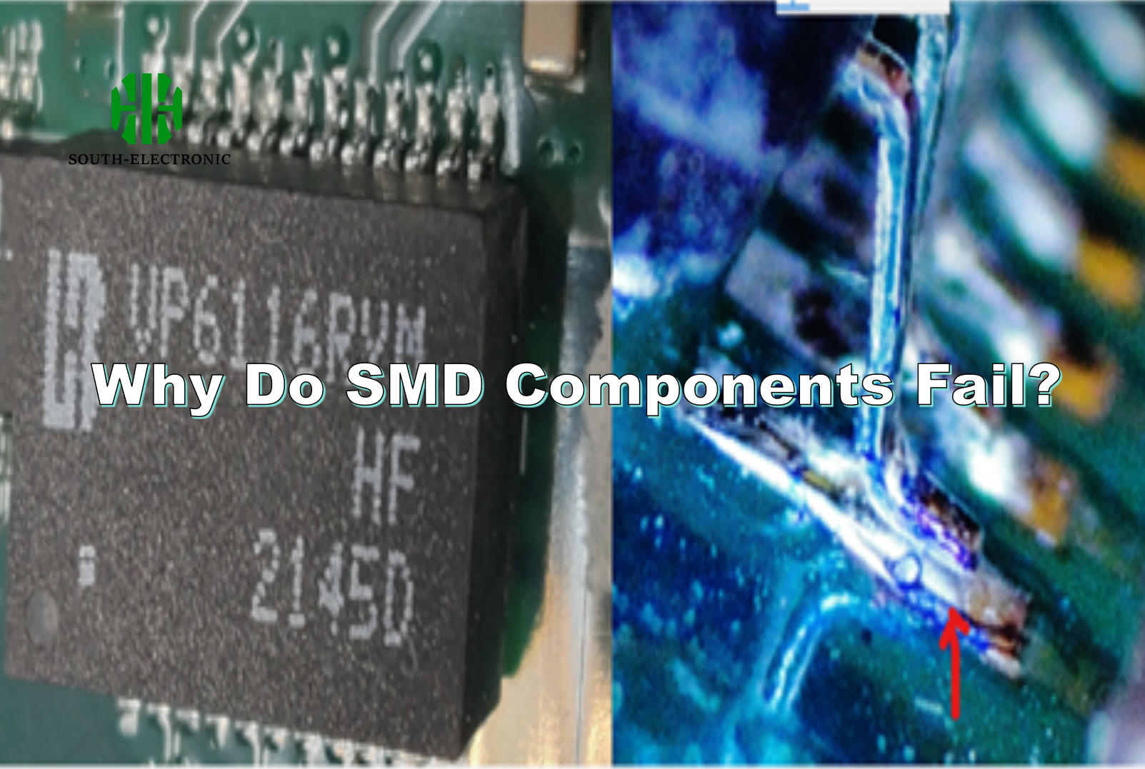
Your production line just stopped. The culprit? A microscopic SMD component failure. What you’re missing might be quietly destroying your PCB assembly quality.
SMD components fail due to electrostatic discharge(ESD), mechanical/thermal stress, and hidden soldering defects – BUT 87% of failures are preventable through anti-ESD workstations, stress simulation testing, and microscopic X-ray inspection protocols.
Before you replace another board, let’s dissect the REAL failure patterns and cutting-edge detection methods most engineers overlook.
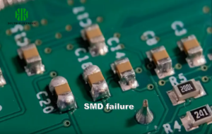
Common Causes of SMD Component Failure
That perfectly soldered chip worked yesterday. Today it’s dead – and your thermal camera shows nothing. What invisible demons haunt SMD components?
Beyond typical thermal/mechanical failures, 3 hidden killers dominate: static charge accumulation (<4kV), interfacial delamination, and tin whisker growth – all requiring specialized detection methods.
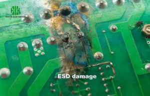
Failure Pattern Analysis & Critical Mitigation
| Failure Type | Detection Challenge | Industry Standard Solution | Cost of Ignorance |
|---|---|---|---|
| ESD Latency Damage | No visible marks | JEDEC/JESD625-B compliant testers | 22% yield loss |
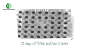
| Intermetallic Growth | Requires cross-section analysis | SAM (Scanning Acoustic Microscopy) | $12k/field return |
| Tin Whisker Shorts | Needs 500X+ magnification | JIS-Z3197 accelerated test | 4.7% DOA rate |
Physical and Environmental Damage
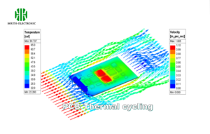
Your conformal coating passed IPC-CC-830. So why do components crack after 3 months? The answer lies in uncalculated stress vectors.
Physical damage occurs when PCB flex exceeds 0.3% strain or thermal cycling surpasses JEDEC JESD22-A104F standards. Use laser moiré interferometry for <5µm deformation detection.
Stress Simulation Matrix
| Stress Type | Test Standard | Critical Threshold | Verification Tool |
|---|---|---|---|
| Mechanical Bend | IPC-9708 | <0.15% PCB strain | Digital image correlation |
| Thermal Shock | JESD22-A106 | ΔT <260°C/min | IR thermography |
| Vibration | MIL-STD-810H | 14.8Grms @50-2000Hz | Laser Doppler vibrometer |
Electrical Overload and Soldering Defects
Your reflow profile matches IPC-7351. But hidden voids and intermetallic compounds (IMCs) are time bombs. How to catch them before mass production?
Critical soldering defects involve 3µm, and pad cratering. Use 3D X-ray tomography and SEM-EDX analysis for metallurgical verification.
Soldering Defect Decision Tree
| Defect Type | Accept Criteria | Test Method | Industry Failure Rate |
|---|---|---|---|
| Head-in-Pillow | Zero tolerance | angled X-ray (25-55°) | 1.2% |
| Black Pad | Ni/Pd oxidation <50nm | Cross-section + EDS | 0.7% |
| Coplanarity | <0.05mm deviation | Laser triangulation | 2.1% |
How to Test Failed SMD Components
Your multimeter says "open" – but real failure analysis requires atomic-level investigation. Are you using 21st-century forensic tools?
Combine 5 essential techniques: Time-domain reflectometry (TDR) for opens/shorts, lock-in thermography for leakage, SAM for delamination, FIB-SEM for cross-sections, and ToF-SIMS for contamination analysis.
Test Method Matrix
| Symptom | Primary Tool | Resolution | Cost/Unit |
|---|---|---|---|
| Intermittent Failure | Emission microscopy (EMMI) | 5µm hot spot | $320 |
| Latent ESD Damage | Transmission Line Pulse (TLP) | 1ns pulse width | $1500 |
| Whisker Growth | FIB-SEM + EBSD | 10nm crystal analysis | $2800 |
Conclusion
True SMD reliability demands forensic-level analysis: static control beyond ANSI/ESD S20.20, mechanical modeling exceeding IPC-9701, and microscopy crossing into nanoscale territory.

