When you’re designing electronics, you might come across unfilled solder points on a PCB (Printed Circuit Board) and wonder what they’re for. These points, which are often overlooked, actually play a critical role in how a circuit functions, how it’s tested, and how it can be designed.
What Are the Unfilled Solder Points on a PCB?

Unfilled solder points on a PCB can serve multiple roles depending on the design and functionality of the board. They can be used for:
- Testing and debugging: These unfilled points are often left open to allow technicians to probe, monitor, and troubleshoot the circuit.
- Alternate layouts: A PCB might be designed to accommodate different versions of a product, meaning unfilled points allow for the inclusion or exclusion of components based on specific model requirements.
- Design changes: Sometimes, a design is modified after PCB production. In such cases, these unfilled points may reflect components that were planned but later excluded due to changes in specifications or design needs.
What Are the Solder Points on a PCB Called?
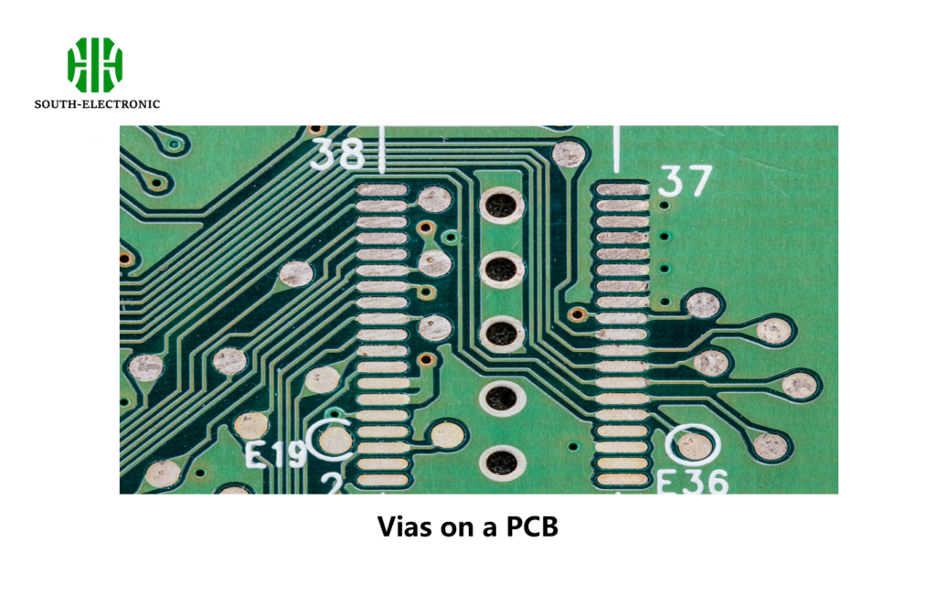
Solder points on a PCB are typically called pads or vias. These small metal areas are where electronic components are attached to the board. There are two main types of solder points:
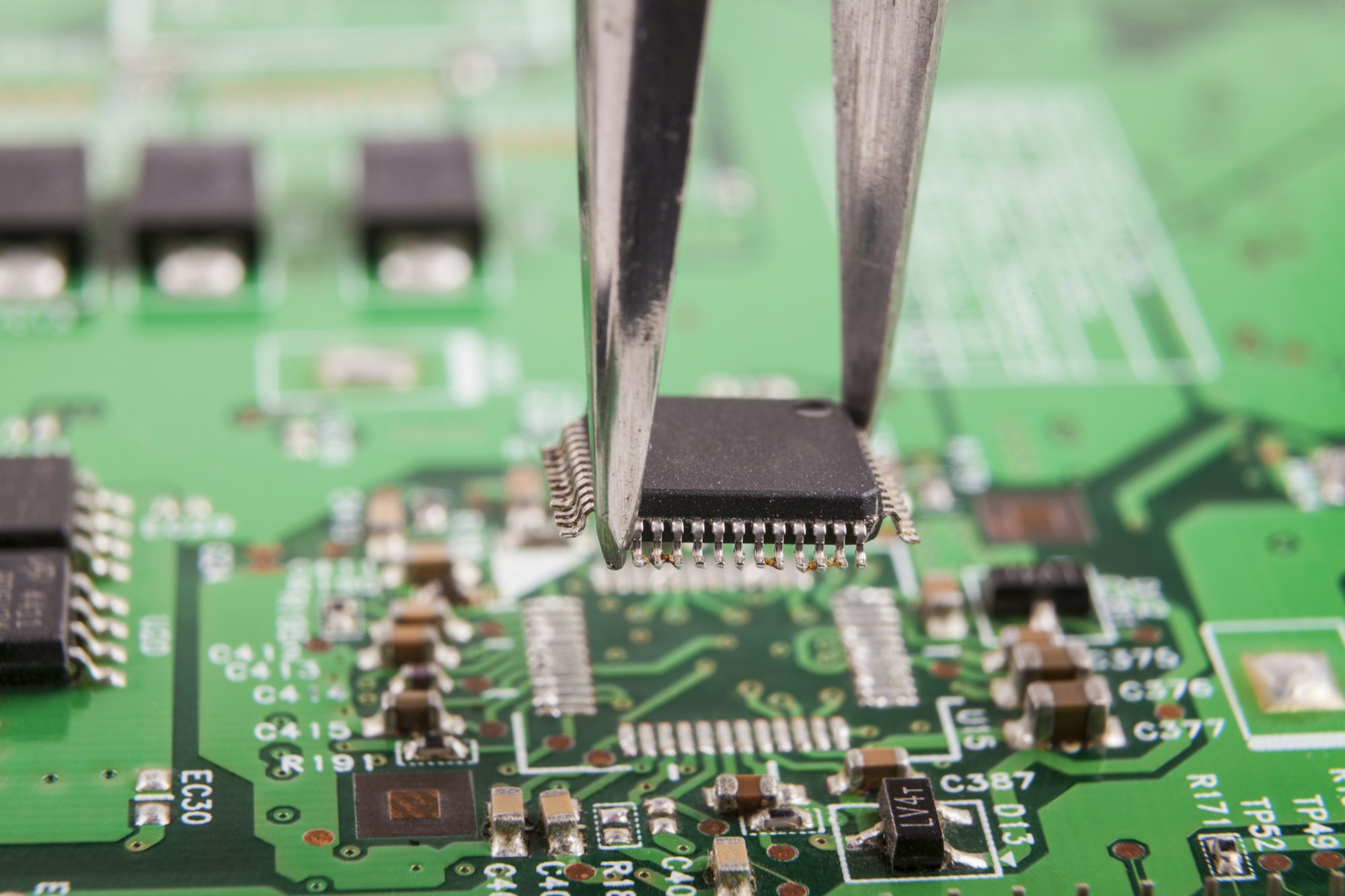
- Surface Mount Devices (SMDs): These components are mounted directly onto the surface of the PCB, and the solder pads on the surface are designed to hold them.
- Thru-Hole Components: These components have leads that pass through the board and are soldered on the opposite side, usually in unfilled vias.
Types of Vias on a PCB
| Type of Via | Description | Use Case |
|---|---|---|
| Plated Thru-Hole | Drilled through the entire PCB to connect all layers | Used in multi-layer PCBs |
| Blind Via | Connects external layers to one or more internal layers | Used for space-saving designs |
| Buried Via | Connects only internal layers, invisible on the surface | Common in compact and complex designs |

What Happens If Unfilled Solder Points Are Ignored?
Not filling solder points can cause problems with circuit operation, especially when you’re testing or debugging. Also, not filling vias can let dirt or moisture collect, which can cause corrosion or shorts.
What Are the Brown Spots on Solder?
The brown spots on the solder joints are usually caused by flux residue. Flux is used during soldering to clean the metal surfaces and ensure a good electrical connection. If it is not properly cleaned, it can leave a discolored residue.
How to Prevent Brown Spots:
- Use Appropriate Flux: Selecting a flux with the correct activation temperature can help prevent residue build-up.
- Proper Cleaning: After soldering, clean the PCB to remove any excess flux that could lead to brown discoloration over time.
Unpopulated solder pads on a PCB may seem like no big deal, but they play important roles in testing, debugging, and enabling alternate layouts. Understanding how unpopulated solder pads contribute to the overall functionality of a PCB helps you make better design and manufacturing decisions, ensuring your circuits are reliable and efficient.


