
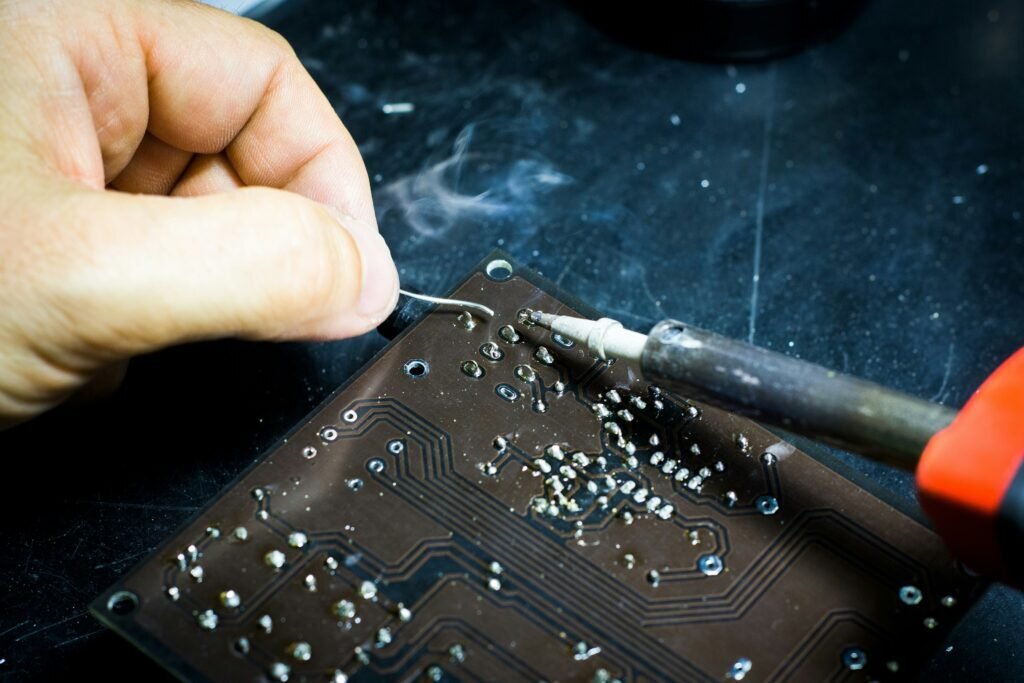
Ever powered on your device only to find smoke or failure? A microscopic solder mistake can kill your entire circuit board instantly. This silent killer ruins projects and budgets without warning.
A solder bridge creates unintended electrical connections causing short circuits that may permanently damage components, disrupt signals, and lead to catastrophic system failure. Identifying bridges early is critical to save repair costs and ensure reliability.
These hidden dangers threaten every electronics project, but solutions exist across design and production stages. I’ve seen boards fail spectacularly over bridges thinner than hair—let’s explore prevention strategies section by section.
How can PCB design prevent solder bridges?
Bad circuit board layouts invite solder bridges. My prototyping disaster proved this: bridges formed between misaligned pins I’d spaced carelessly. Panic set in when the microcontroller fried instantly.
Expand pad spacing beyond manufacturer minimums, use solder mask dams between pins, and avoid right-angle traces near ICs. Add thermal reliefs in ground planes to control solder flow during reflow. Review designs using DFM software.
Critical design adjustments
Three factors dominate bridge prevention at the design stage: spacing, barriers, and heat control.
| Design Factor | Purpose | Implementation Example |
|---|---|---|
| Component Spacing | Prevents overflow merging | 0.5mm gap between QFP pins |
| Solder Mask | Creates physical barriers | 5mil dams between BGA pads |
| Thermal Balance | Avoids uneven melting | Symmetrical pad heating zones |
Small gaps between surface-mount pads risk solder merges during reflow. My rule: space pins 30% wider than datasheet minimums. Solder mask isn’t decoration—it chemically resists bridges between pins like tiny dams. Thermal reliefs in copper pours stop heat traps that make uneven melting.
What is a solder bridge jumpe?
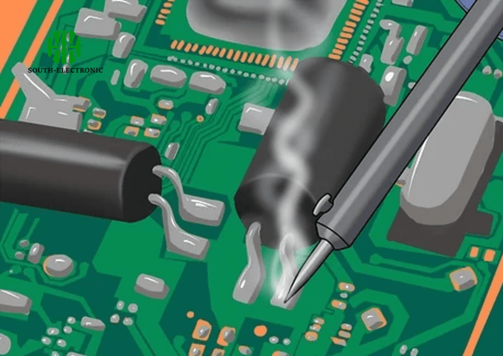
A "solder bridge jumper" signals design failure. I created one accidentally while reworking a Bluetooth module—my shaky soldering tip blobbed pins together. Surprisingly, the device worked until thermal stress broke it.
A solder bridge jumper is an unintentional conductive path between separate circuit points, functioning like an electrical shortcut that bypasses designed pathways. Although rarely functional, temporary jumps can create misleading behaviors before breakdown.
Failure progression analysis
Bridge jumpers evolve through distinct failure phases:
| Stage | Characteristics | Risks |
|---|---|---|
| Formation | Microscopic connection | Intermittent operation |
| Operation | Partial current leakage | Component overheating |
| Failure | Thermal damage/scorching | Permanent board destruction |
Initially microscopic, bridging expands with thermal cycles like repeated device use. Acting as an unauthorized conductor, it redirects current away from intended paths. Components starved of correct current may underperform while the bridge point overheats. Eventually, the thin bridge material vaporizes—often catastrophically. This explains why devices with hidden bridges sometimes seem functional initially.
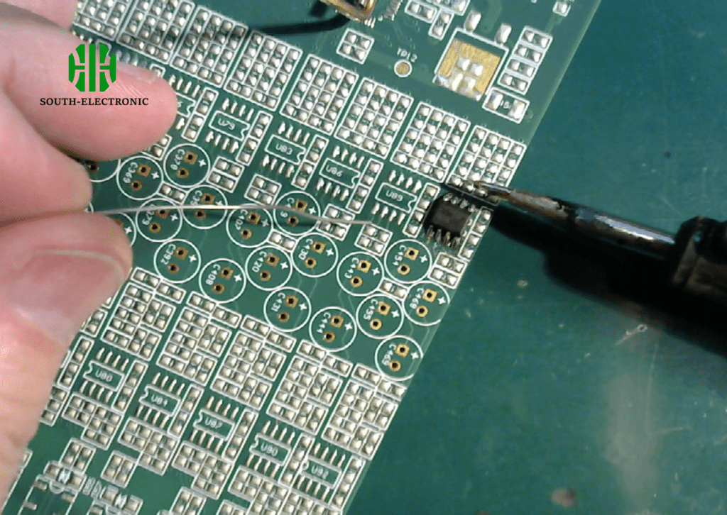
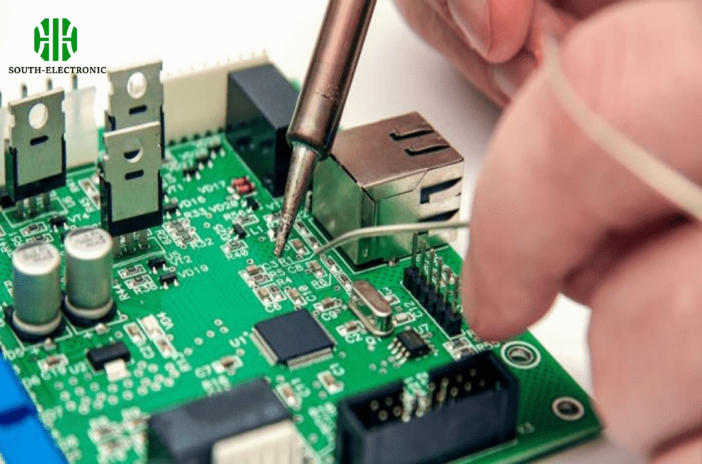
How to avoid solder bridges during assembly by optimizing manufacturing and process?
Assembly lines create bridges from rushed processes. A factory once overlooked stencil cleaning—solder paste clogging caused rampant bridges. I saw 23% yield drop in two hours until they fixed it.
Control paste volume with stencil thickness checks, maintain exact reflow oven profiles, and enforce automated optical inspection. Clean pads before assembly and verify component alignment—0.05mm shifts can cause bridging.
Assembly parameter optimization
Key variables require constant monitoring:
| Parameter | Ideal Range | Effect if Uncontrolled |
|---|---|---|
| Paste Volume | 80-85% pad coverage | Overflow causes bridges |
| Reflow Peak Temp | 235-245°C | Low temp traps viscosity |
| Placement Accuracy | ±0.1mm | Misalignment enables bridging |
Stencil wiping cycles become critical—uncleaned apertures deposit excess paste. Reflow oven zones need daily validation; uneven heating keeps solder liquid too long, letting it crawl between pins. Automated inspection systems must flag even micro-bridges human eyes miss.
Conclusion
Solder bridges trigger irreversible circuit failure but vanish through strategic PCB design and disciplined assembly. Immediate prevention always beats expensive post-mortem repairs.


