
PCB defects cause expensive recalls. Faulty electronics ruin brand trust instantly. Automated optical inspection catches errors early for quality control.
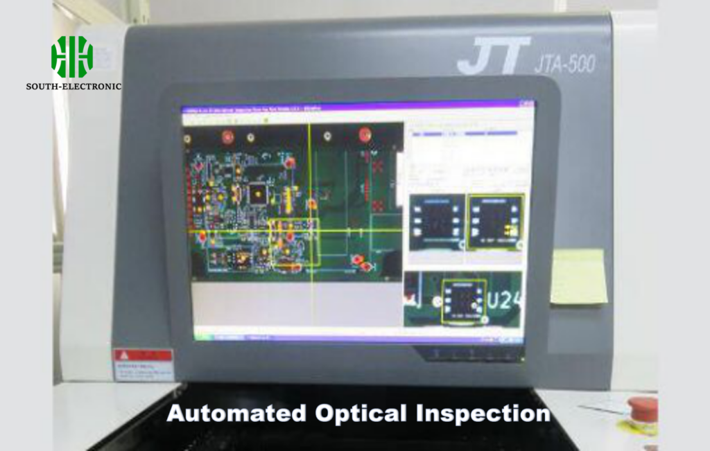
AOI is critical because it detects component placement errors and soldering defects automatically during production. This prevents costly rework and ensures reliable electronics reach customers quickly and safely.
Understanding AOI value opens doors to smarter implementation. Now let’s resolve key selection puzzles blocking your efficiency gains.
Which technology fits your production line: 2D or 3D AOI systems?
Wrong AOI picks waste money. Limited vision systems miss critical defects. Match technology to your actual product needs.
2D suits flat component inspection with lower cost. 3D handles complex shapes and height variations precisely but requires higher investment. Product complexity decides the winner.
Key Factors for Selection
Production volume and defect types determine ideal AOI systems. High-mix factories need flexibility while mass producers prioritize speed.
Technology Comparison Table
| Inspection Need | 2D AOI Strength | 3D AOI Advantage |
|---|---|---|
| Component Placement | Good for basic ICs | Excellent for BGAs & QFNs |
| Solder Joint Quality | Limited visibility | Precise height measurement |
| Cost Efficiency | Lower initial investment | Higher long-term ROI |
| Speed | Faster scanning | Moderate throughput |
| False Call Rate | Higher without height data | Lower through 3D analysis |
Budget matters but shouldn’t override technical needs. One automotive manufacturer cut field failures 30% after switching to 3D for micro-BGA inspection. Always analyze your defect patterns first before choosing cameras or software.
Can AI reduce false calls in AOI?
False alarms slow production. Operators lose trust in AOI alerts. Wasted rework time kills shop floor efficiency fast.
AI learns from past mistakes. This smart algorithm separates real defects from shadows or reflections. Your team stops chasing ghost problems.

Reducing False Calls Step-by-Step
Training data teaches AI systems over time. Initial setup requires historical defect images to establish baseline judgment patterns.
Implementation Stages
-
Data Collection Phase
Gather 200-500 images of known good/bad boards -
Algorithm Training
Machine learning identifies subtle defect patterns -
Testing Cycle
System accuracy validated against human inspectors -
Continuous Learning
Regular updates improve detection rates monthly
Each stage reduces false alarms incrementally. A medical device maker reported 47% fewer false alerts after six months of AI refinement. Patience during calibration pays off with major productivity gains.
How to optimize your inspection strategy investment with AOI, SPI, or AXI?
Money spent wrongly hurts profits. Standalone tools create inspection gaps. Combine technologies at strategic points for full coverage.
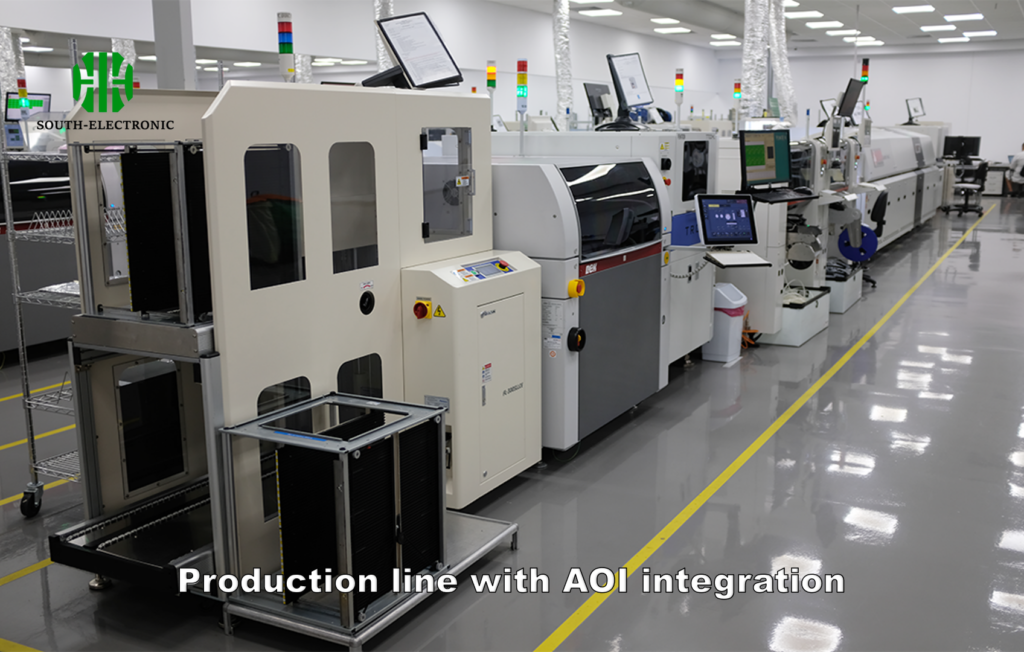
SPI checks solder paste before placement. AOI inspects component assembly after reflow. AXI examines hidden solder joints under chips. Together they form complete defect shields.
Building a Cost-Efficient Strategy
Prioritize failure points affecting your products most. Budget allocation depends on component sensitivity.
Inspection Technology Capabilities
| Process Stage | Ideal Tool | Defects Caught |
|---|---|---|
| Post-Solder Paste | SPI | Paste volume/alignment errors |
| Post-Pick & Place | AOI | Missing/wrong components |
| Post-Reflow | AOI/AXI combo | Lifted leads, tombstoning, hidden shorts |
| Final Assembly | AXI/X-ray | Internal BGA connections, voids |
A consumer electronics company slashed defect escape rates by 65% through tiered spending: budget AOI units at reflow zones and shared AXI stations after final assembly. Never allocate equal money – match tools to risk hotspots.
Conclusion
AOI prevents defects escaping production. Choosing the right technology stack builds quality control shields while maximizing investment returns across assembly stages.

