

Circuit boards form the backbone of modern electronics and often face reliability challenges in demanding conditions.
FR4 dominates PCB manufacturing because it offers the best balance of affordability, robustness, insulation properties, and fire safety for everyday electronics. This glass-reinforced epoxy material meets UL94 V-0 flame standards while providing stable electrical performance across temperatures, making it ideal for cost-sensitive projects.

Now, let’s explore specific aspects that make FR4 universally trusted across industries. Understanding these details helps avoid design failures.
What is the TG value in FR4 PCBs?
Most hobbyists overlook glass transition temperature, risking board failure under heat.
Tg indicates when FR4 changes from rigid to rubbery state; standard FR4 has 130-140°C Tg, while high-Tg versions (170°C+) withstand harsh environments better. This value ensures stable signal integrity and physical shape during soldering or high-power operation.
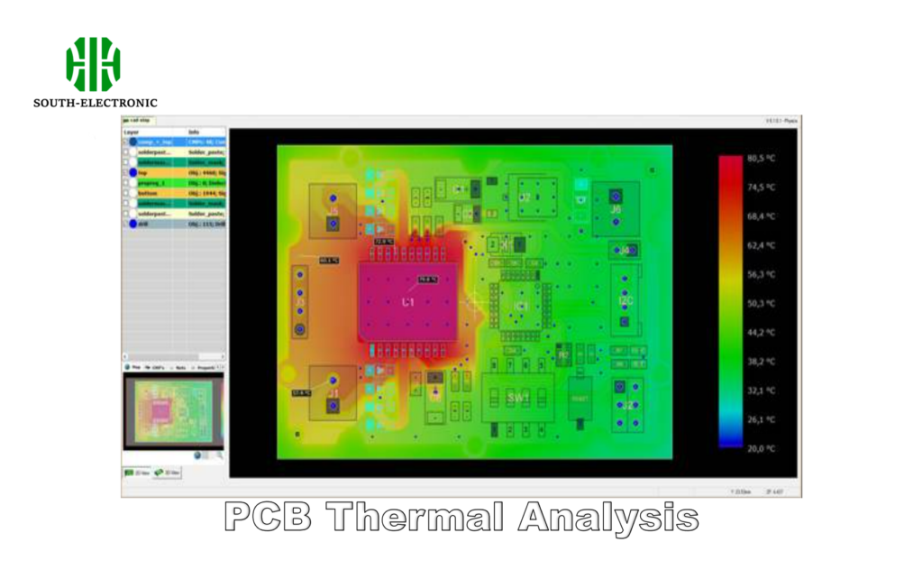
Why Tg Matters for Reliability
Critical applications expose boards to heat cycles that warp low-Tg material. For example:
- Automotive/industrial systems need >150°C Tg to survive engine heat
- High-speed circuits demand material stability to maintain impedance
| Tg Range | Use Cases | Risks If Ignored |
|---|---|---|
| 130-140°C | Consumer gadgets, IoT devices | Delamination under reflow |
| 150-170°C | Power supplies, LED lighting | Warping near heat sinks |
| 180°C+ | Aerospace, military systems | Trace cracking in extreme cold |
Material selection mistakes cause irreversible damage – I once saw a drone controller fail mid-flight when generic FR4 warped near motors. Higher Tg costs 10-20% more but prevents field failures. Always verify supplier datasheets since "FR4" includes various formulations with different thermal capabilities. Humidity absorption also drops with increased Tg, protecting against corrosion.
What FR4 PCB design rules should not be ignored?
Rushed PCB layouts often waste weeks fixing avoidable production issues.
Always define minimum trace width/spacing early (typically 6/6 mils standard) while avoiding 90° trace angles to prevent acid traps during etching. Copper planes need thermal reliefs to ease soldering without compromising heat dissipation.
Critical Design Checks
Overlooked constraints escalate costs exponentially:
- Impedance control: Match trace widths to FR4’s Dk value (typically 4.5). This matters for RF/high-speed circuits
- Edge clearances: Maintain >40 mils from board edges for mechanical milling stability
- Drill hole size – Pads must be 8 mils larger than drilled holes to avoid breakout
| Rule Type | Standard Value | Why It Matters |
|---|---|---|
| Minimum Trace Width | 6 mil | Prevents open circuits |
| Copper-to-Edge Spacing | 40 mil | Avoids cracking during assembly |
| Solder Mask Expansion | 4 mil | Ensures pad coverage |
Neglecting these caused my prototype batch to short – acid trapped in sharp corners eroded copper. Manufacturers also penalize small via holes (5 seconds blisters low-Tg FR4
| Risk Area | Solution | Cost of Failure |
|---|---|---|
| Drill Wear | Replace bits every 500 hits | Broken vias ($200/board) |
| Moisture Absorption | Pre-bake at 120°C for 4 hours | Popcorning during reflow |
| Oxide Treatment | Use alternative surface finishes | Poor solder adhesion |
I learned these lessons after a 100-board batch delaminated – moisture in the FR4 expanded during reflow. Use lead-free HASL or ENIG finishes; cheap HASL melts at 300°C and risks board warping. Partner tightly with fabricators since FR4 suppliers change resin formulas marginally but functionally.
Conclusion
FR4 delivers unparalleled price-performance harmony for PCBs, but respecting its design boundaries prevents costly errors. Always validate material specs with your application.

