What is a Double-Sided Motherboard?
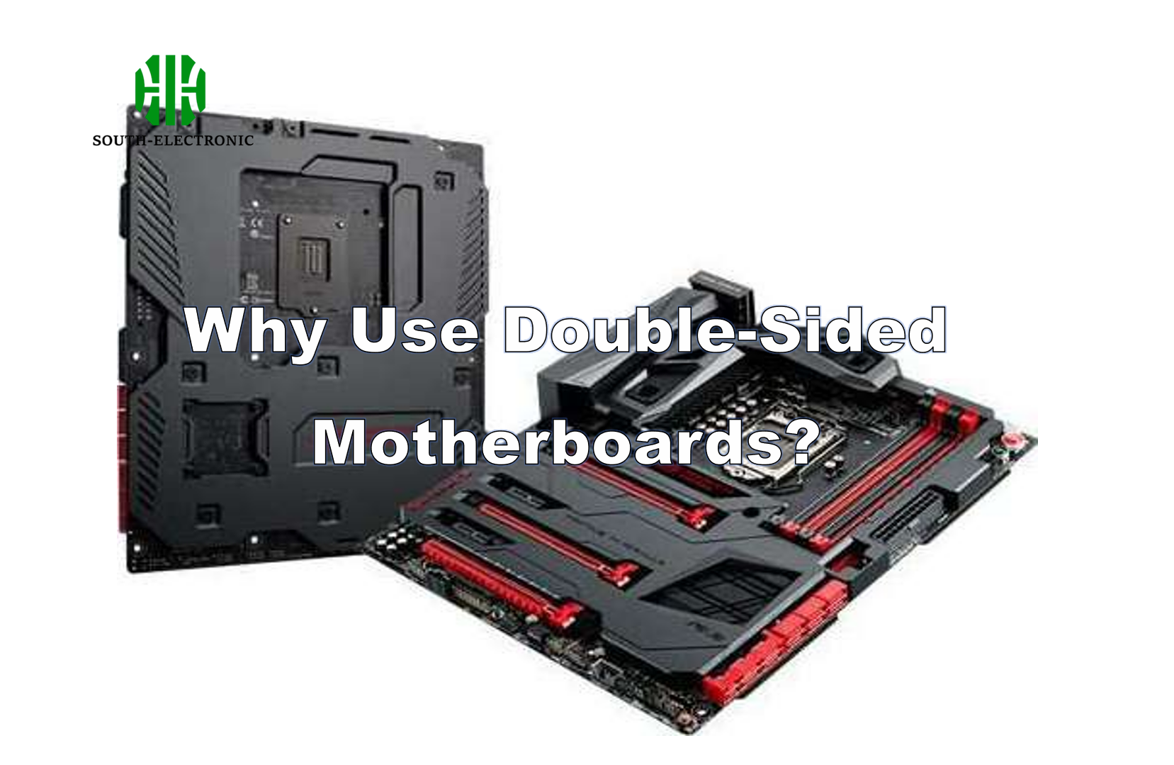
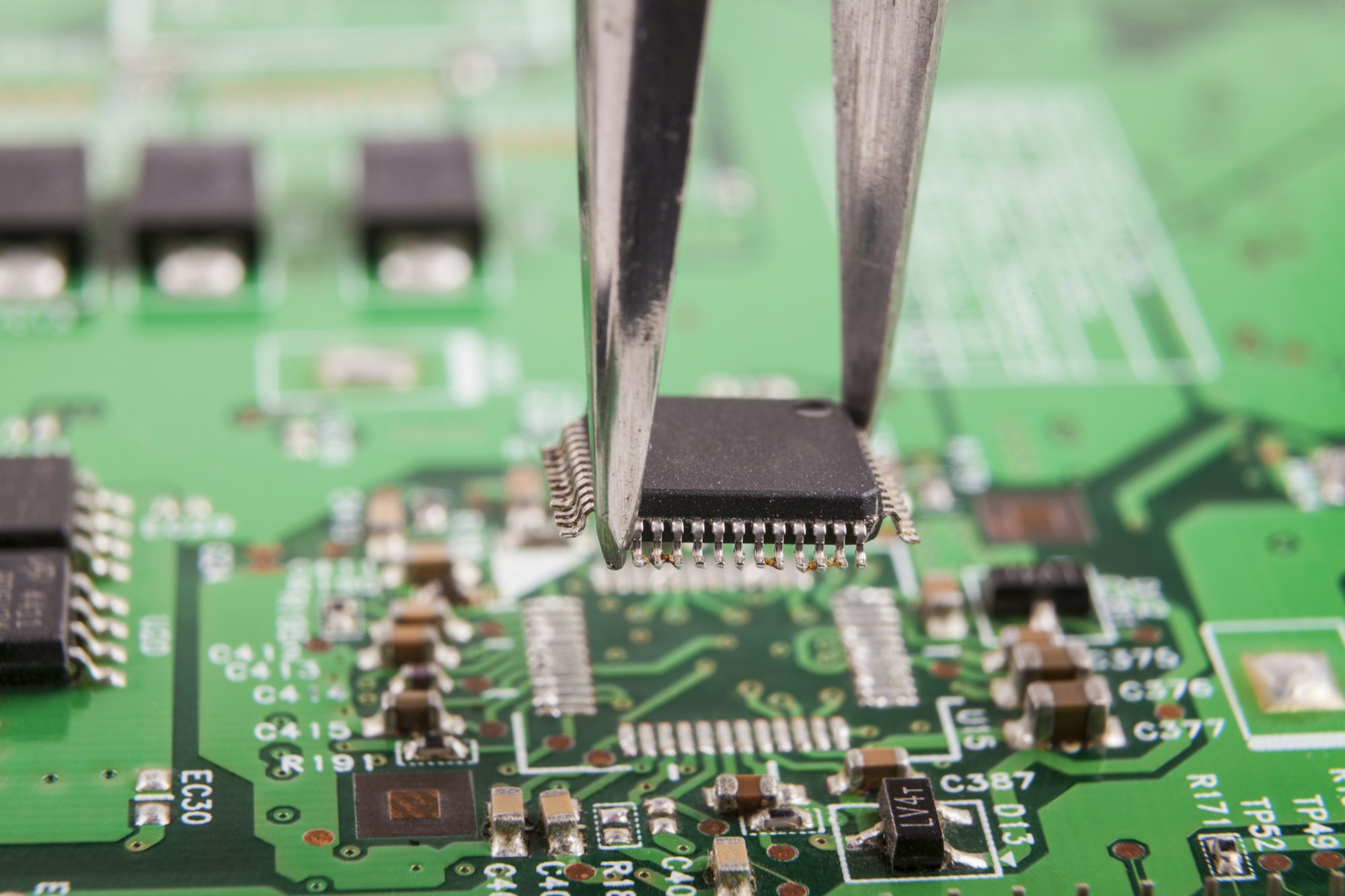
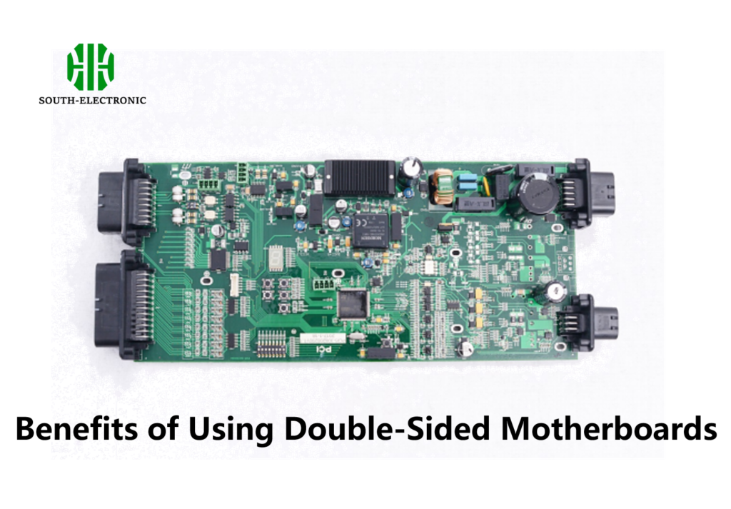
A double-sided motherboard, or double-sided printed circuit board (PCB), refers to a board that has conductive layers on both sides. This design allows for the placement of components on both surfaces, significantly increasing circuit density and efficiency. Double-sided motherboards are essential in modern electronics where compactness and performance are vital, making them ideal for everything from consumer gadgets to advanced industrial devices.
How Does a Double-Sided PCB Work?
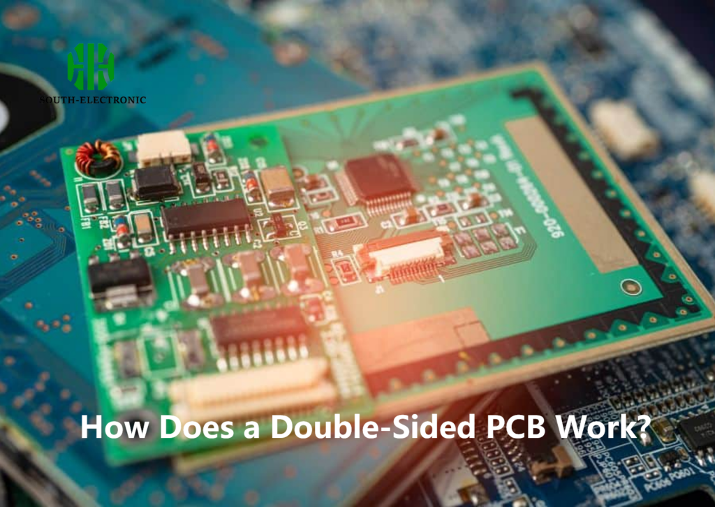
The core functionality of a double-sided PCB lies in its ability to connect circuits across both layers of the board. This is achieved using vias, tiny holes that allow electrical connections to pass through the board, linking the top and bottom copper layers.
Key Components of a Double-Sided PCB:
- Copper Traces: The conductive pathways on both sides of the board.
- Vias: Small holes that allow electrical signals to travel between the two layers.
- Dielectric Layer: The insulating material between the two conductive layers.
- Solder Mask: Protective layer that prevents short circuits.
Single-Sided vs. Double-Sided PCB: Key Differences
| Feature | Single-Sided PCB | Double-Sided PCB |
|---|---|---|
| Component Placement | Only on one side | Components can be placed on both sides |
| Circuit Complexity | Limited | More complex circuits possible |
| Cost | Lower cost | Higher manufacturing cost |
| Application | Simple electronics | Advanced electronics |
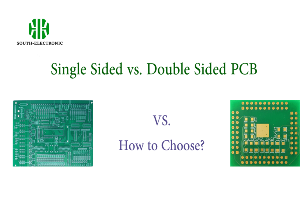
A single-sided PCB only has conductive copper on one side, limiting the number of components and complexity of circuits. On the other hand, a double-sided PCB allows for more efficient use of space and enhanced circuit performance, which is why it’s preferred in more advanced devices.
Benefits of Using Double-Sided Motherboards
There are several advantages to using double-sided motherboards in modern electronics:
1. Increased Circuit Density
Double-sided motherboards offer a higher component density, allowing engineers to pack more functionality into a smaller board. This is particularly useful in compact devices like smartphones and tablets.
2. Improved Performance
With more space for routing, double-sided PCBs can support faster and more efficient circuits, resulting in improved device performance.
3. Flexibility in Design
The ability to use both sides of the board offers more flexibility when designing circuits. Engineers can cross traces more easily, reducing the risk of interference and signal degradation.
Challenges of Manufacturing Double-Sided PCBs
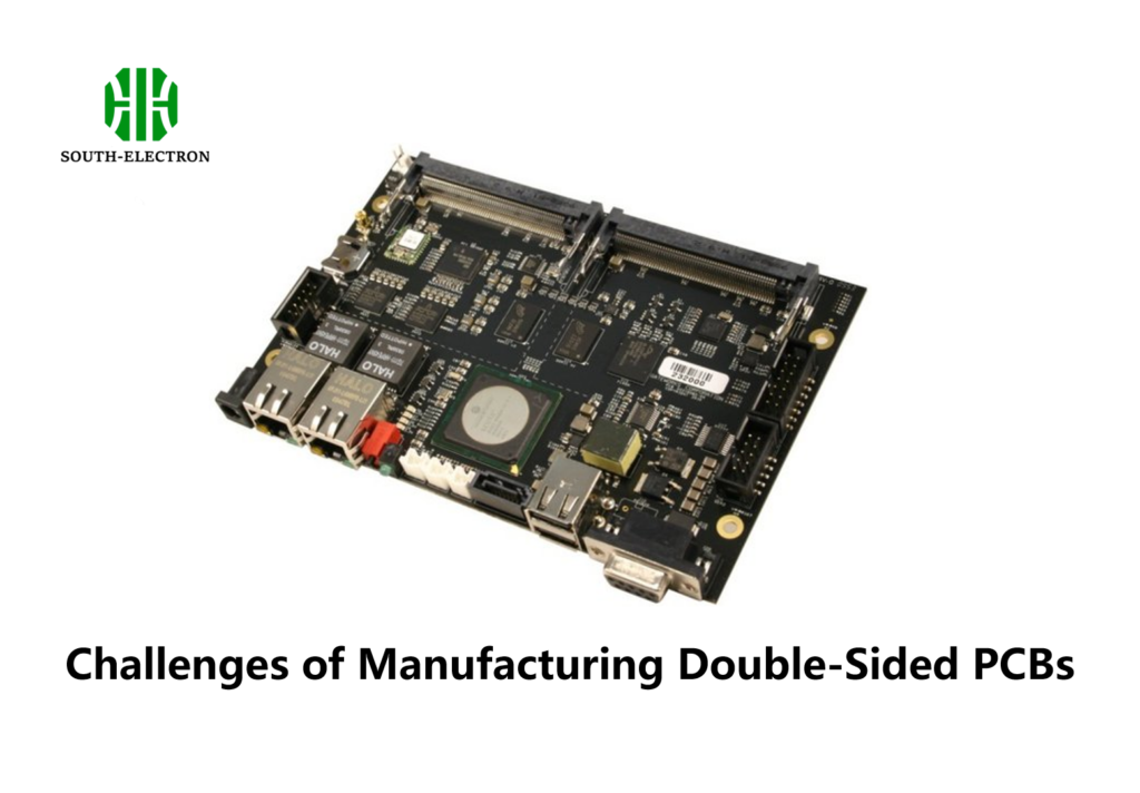
Manufacturing double-sided PCBs is more complex than single-sided boards due to the need for precise alignment between the two layers. Here are some key challenges:
1. Alignment and Vias
Proper alignment of vias and traces is critical to ensure that signals can pass between the top and bottom layers without issues.
2. Higher Costs
Double-sided boards are more expensive to produce due to the additional layers and complexity involved in the manufacturing process.
Double-Sided PCB Advantages and Disadvantages
| Aspect | Advantages | Disadvantages |
|---|---|---|
| Component Density | Supports higher circuit density and complexity | More difficult to manufacture |
| Cost Efficiency | Cost-effective for advanced applications | Generally higher cost than single-sided PCBs |
| Space Efficiency | Allows for compact designs, critical in consumer devices | Potential for thermal issues due to higher component density |
| Signal Integrity | Reduced interference by allowing flexible routing | Harder to repair or modify once assembled |
Double-sided PCBs strike a balance between functionality and cost, making them a popular choice for mid- to high-complexity electronics.
Double-Sided PCB vs. Multilayer PCB: Which is Better?
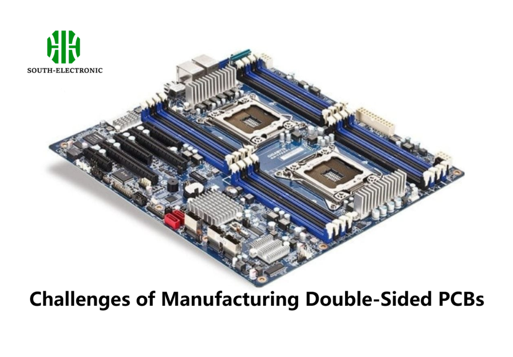
While double-sided PCBs allow for components and copper traces on both sides of the board, multilayer PCBs take it a step further by incorporating multiple layers of copper separated by insulating material. Multilayer boards are ideal for even more complex circuits, such as those found in servers and advanced computing systems.
Key Differences:
- Double-Sided PCB: More affordable, easier to manufacture, and sufficient for most consumer electronics.
- Multilayer PCB: Suitable for highly complex, high-performance devices, but with a significant increase in cost and manufacturing difficulty.
Double-sided motherboards are a key innovation in the electronics industry, allowing for high circuit density, flexibility in design, and improved performance across a wide range of applications. From consumer gadgets to industrial machinery, double-sided PCBs will continue to play a vital role in advancing technology.

