
This article will explain in detail the construction of PCBs, common terminology used in the PCB field, a brief introduction to assembly methods, and an overview of the PCB design process.
The Birth of PCBs
Before the advent of PCBs, circuits were constructed using point-to-point wiring. This method was highly unreliable because, as circuits aged, cracks in the wiring could cause disconnections or shorts at circuit nodes.
Wire wrapping was a major advancement in circuit technology. This method improved the durability and replaceability of circuits by wrapping small-diameter wire around posts at connection points.

As the electronics industry evolved from vacuum tubes and relays to silicon semiconductors and integrated circuits, the size and price of electronic components decreased.
The increasing frequency of electronic products in the consumer market prompted manufacturers to seek smaller and more cost-effective solutions, leading to the birth of PCBs.
The Components of PCBs
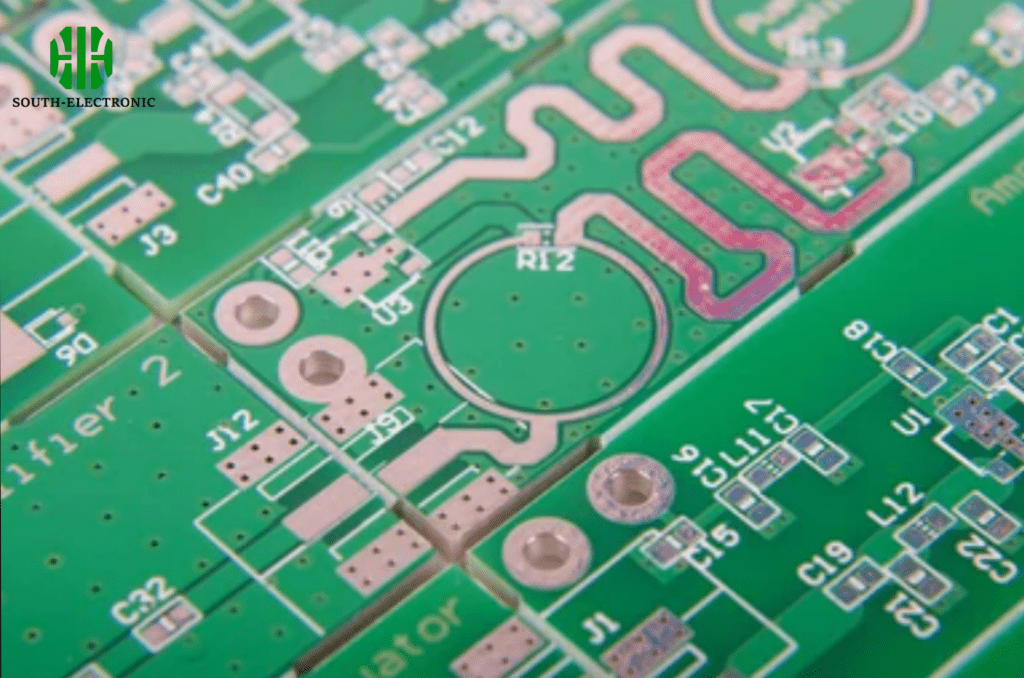
PCBs resemble layer cakes or lasagna—layers of different materials are bonded together using heat and adhesives.
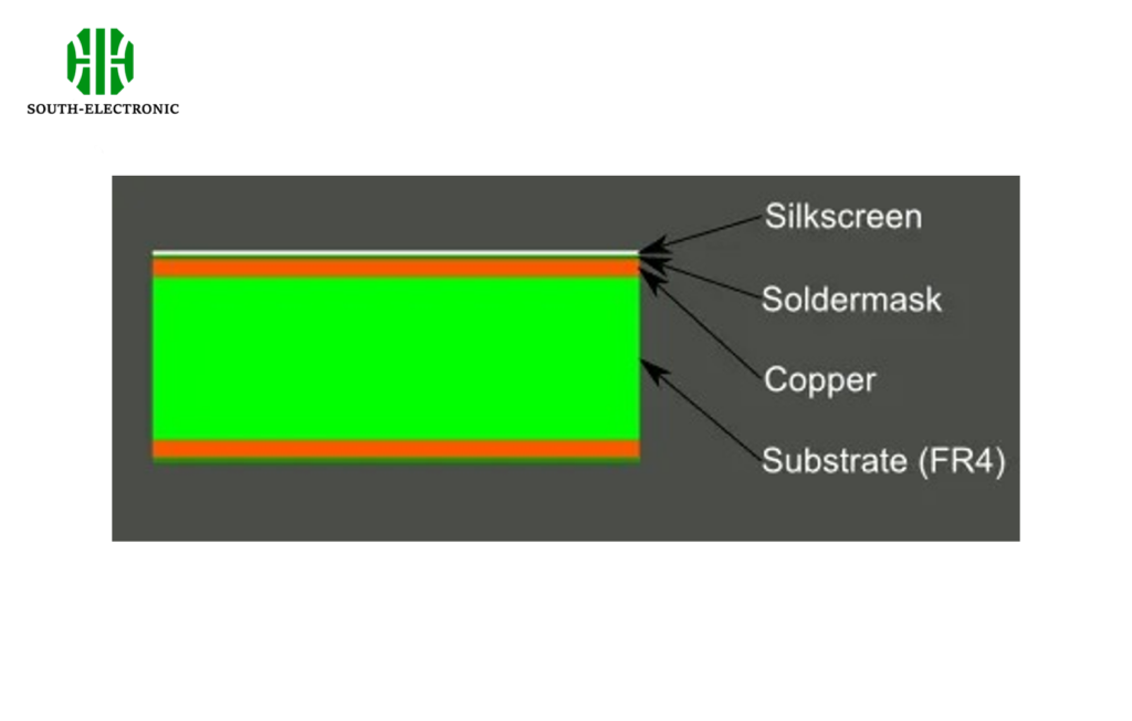
PCB Base Material
The base material of a PCB is generally fiberglass. In most cases, this fiberglass base material refers to FR4. This solid material gives the PCB its rigidity and thickness.
In addition to FR4, there are also flexible circuit boards made from flexible, high-temperature plastics (polyimide or similar).
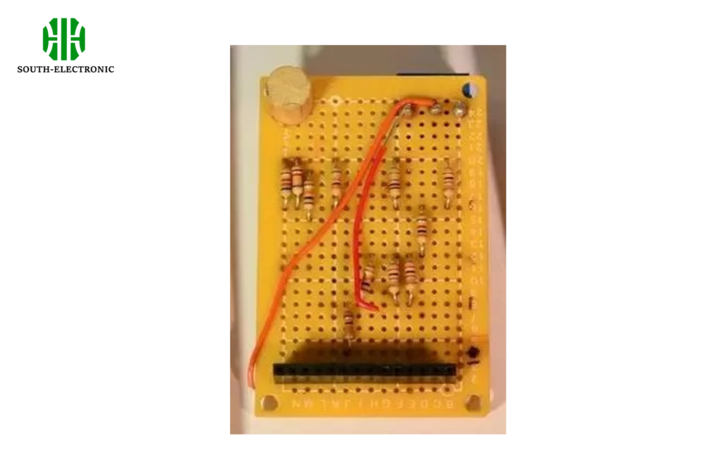
Cheap PCBs and perfboard (see the image above) are made from materials like epoxy or phenolic. They lack the durability of FR4 but are much cheaper. When soldering on these boards, a strong odor will be detected.
This type of base material is often used in very low-end consumer products. Phenolic materials have a low thermal decomposition temperature. Prolonged soldering time will cause them to decompose and carbonize, emitting an unpleasant odor.
Copper Foil

Next, we will introduce a very thin layer of copper foil. During production, it is laminated to the base material using heat and adhesive. On double-sided boards, the copper foil is laminated to both sides of the base material. In some low-cost applications, copper foil may only be laminated on one side of the substrate. When we refer to a "double-sided board" or "two-layer board," we’re referring to two layers of copper foil.
Of course, different PCB designs may have as few as one copper layer or as many as 16.
Copper thickness varies widely and is measured in weight, typically expressed in ounces (oz) per square foot.
Most PCBs have a copper thickness of 1oz, but some high-power PCBs may use 2oz or 3oz. Converting ounces (oz) per square foot to a copper thickness of approximately 35µm or 1.4mil.
Solder Mask
Over the copper layer is the solder mask, which gives the PCB its green or SparkFun red color.
The solder mask covers the traces on the copper layer, preventing shorts from coming into contact with other metals, solder, or other conductive materials. The solder mask ensures soldering is performed in the correct locations and prevents solder bridging.
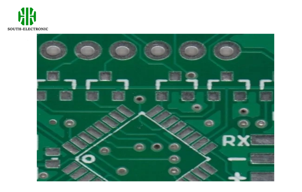
As shown in the image above, the solder mask covers most of the PCB, including the traces, but leaves the silver annular ring and SMD pads exposed for easy soldering. Typically, solder mask is green, but almost any color can be used.
Silkscreen
Above the solder mask is the white silkscreen. Letters, numbers, and symbols are printed on the silkscreen of the PCB to facilitate assembly and provide guidance for understanding the board design.
We often use symbols on the silkscreen to indicate the function of certain pins or LEDs. While white is the most common color, silkscreen can be almost any color.
Black, gray, red, and even yellow silkscreen are not uncommon, but it’s rare to see multiple silkscreen colors on a single board.

