
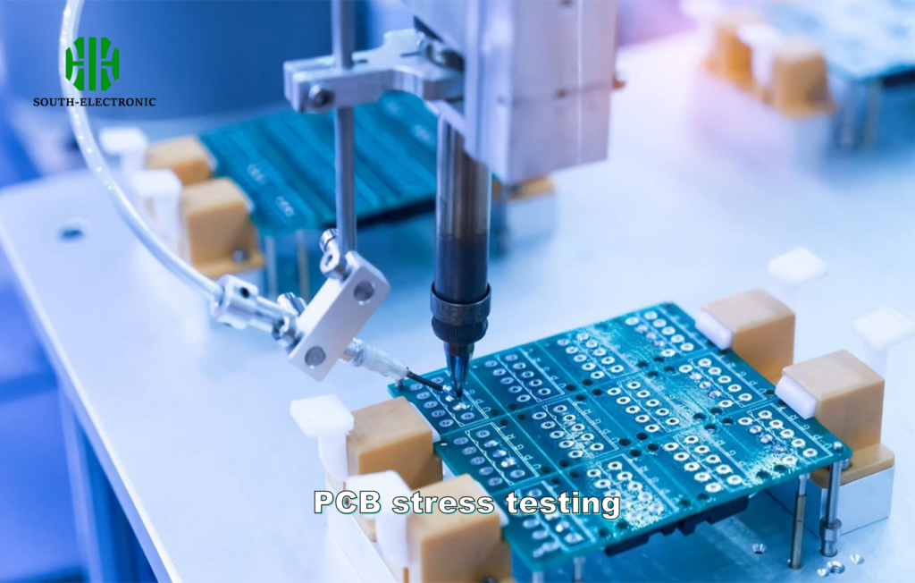
Printed circuit boards (PCBs) are widely used in a variety of electronic devices, from mobile phones and computers to complex machines. If a PCB has defects or manufacturing issues, it can lead to malfunctions in the final product and cause inconvenience. In these cases, manufacturers will have to recall the equipment and spend more time and resources to repair the problem.
Therefore, PCB testing has become an indispensable part of the circuit board manufacturing process, identifying problems promptly and enabling rapid resolution, thereby ensuring high-quality PCBs.
Let’s take a look at 13 common PCB testing methods.
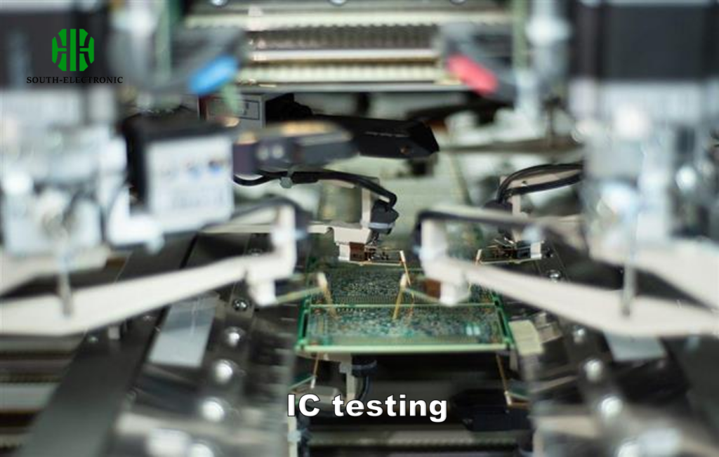
1. In-Circuit Testing (ICT)
ICT, or automated in-circuit testing, is a powerful and essential testing tool for modern PCB manufacturers. It primarily uses test probes to contact test points on the PCB layout to detect opens, shorts, and other component failures on the PCBA, clearly notifying the operator.
ICT has a wide range of applications, high measurement accuracy, and clear indication of detected problems, making it easy for even workers with average electronics skills to troubleshoot problematic PCBAs. Using ICT can significantly improve production efficiency and reduce production costs.

2. Flying Probe Test
Both flying probe testing and in-circuit test (ICT) are well-established and effective testing methods, both effectively identifying production quality issues. However, flying probe testing has proven to be a particularly cost-effective method for improving PCB standards.
In contrast to traditional test methods where test probes are fixed in position, flying probe testing uses two or more independent probes, operating without fixed test points. These probes are electromechanically controlled and move according to specific software instructions. Therefore, flying probe testing has a lower initial cost and can be performed through software modifications without changing the fixed structure. In contrast, ICT has higher initial fixture costs, making flying probe testing less expensive for small-volume orders. However, ICT is faster and less error-prone than flying probe testing, making it more cost-effective for large-volume orders.
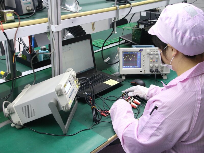
3. Functional Testing
Functional system testing uses dedicated test equipment at the mid- and end-of-line stages to thoroughly test the functional modules of a PCB to confirm its quality. Functional testing primarily includes final product testing and hot mock-up testing.
Functional testing generally does not provide in-depth data (such as pin location and component-level diagnostics) to improve processes. Instead, it requires specialized equipment and specially designed test programs. Writing functional test programs is complex and therefore unsuitable for most PCB production lines.
4. Automated Optical Inspection (AOI)
AOI uses a single 2D camera or two 3D cameras to take a picture of the PCB and then compares it to a detailed schematic. If the board does not match the schematic to a certain extent, the discrepancy is flagged for inspection by a technician, allowing AOI to detect faults promptly.
However, AOI does not power the board and cannot detect 100% of component defects. Therefore, AOI is often used in conjunction with other test methods. Common test combinations include: AOI and flying probe testing.
-
AOI and in-circuit testing (ICT)
-
AOI and functional testing

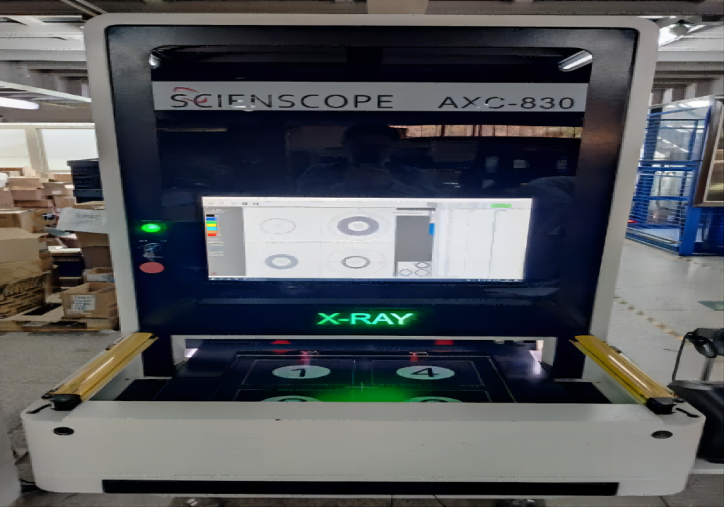
5. X-ray testing
X-ray testing, also known as X-ray inspection, uses low-energy X-rays to quickly detect issues such as opens, shorts, open solder joints, and missing solder joints on PCBs.
X-ray is primarily used to detect defects in ultra-fine pitch and ultra-high density circuit boards, as well as defects such as bridging, missing chips, and misalignment that occur during the assembly process. It can also use tomography to detect internal defects in IC chips. It is the only method for testing ball grid arrays and solder ball bond quality. Its main advantage is that it can inspect BGA solder quality and embedded components without the expense of fixtures.
6. Laser Inspection
This is the latest development in PCB testing technology. It scans the printed circuit board with a laser beam, collects all measurement data, and compares the actual values with preset acceptance limits. This technology has been proven on bare boards and is being considered for testing assembled boards. Its speed is sufficient for mass production lines. Its main advantages are fast output, the absence of fixtures, and unobstructed visual access. Its main disadvantages are high initial cost and maintenance and usage issues.
7. Burn-in Testing
Burn-in testing is the process of conducting intensive testing under conditions that simulate the various factors encountered in real-world use, causing product aging. The purpose is to test the stability and reliability of the product under specific conditions.
Based on design requirements, the product is placed under specific temperature and humidity conditions for 72 hours to 7 days of simulated operation. Performance data is recorded and used to reverse engineer improvements during the production process to ensure that performance meets market demand. Burn-in testing typically refers to electrical performance testing. Similar tests include drop testing, vibration testing, and salt spray testing.
In addition to the seven tests mentioned above, other testing methods may be used to further ensure PCB quality based on product requirements. As follows:
8. Solderability Testing
Ensures a strong surface and increases the chances of forming reliable solder joints
9. PCB Contamination Testing
Detects large amounts of ions that can contaminate the board, causing corrosion and other problems
10. Microsection Analysis
Investigates defects, opens, shorts, and other faults
11. Time Domain Reflectometry (TDR)
Discovers faults in high-frequency boards
12. Peel Testing
Determines the strength required to peel the laminate from the board
13. Solder Float Testing
Determines the level of thermal stress a PCB hole can withstand
PCBA testing is an essential process that, if done correctly, can prevent quality issues that can damage your brand when your product reaches market.

