

Growing circuit complexity demands smarter PCB stacking strategies. Failed stack-up designs lead to signal distortion, EMI nightmares, and thermal disasters. I’ll show you how to combine physics and geometry into functional multilayer solutions.
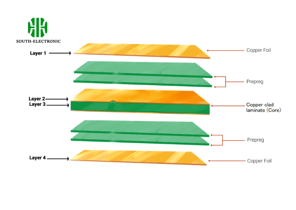
Multilayer PCB stack-up construction[^1] requires strategic layer sequencing, material compatibility analysis, and EMI mitigation planning[^2]. Key steps include determining layer count based on circuit complexity, selecting dielectric materials for signal integrity, and arranging copper layers with proper shielding.
Every layer decision impacts cost, performance, and manufacturability. Let’s break down critical design choices through four fundamental questions.
What Factors Determine the Optimal Number of Layers in a Multilayer PCB?
Engineers often underestimate layer count requirements early in design. Inadequate layers force signal compromises while excessive layers inflate costs needlessly.
Layer count depends on signal types[^3] (high-speed/RF/digital), required impedance control, power delivery needs, and thermal dissipation requirements. Four-layer boards handle basic designs, while 12+ layers manage complex BGAs and mixed-signal systems.
Layering Decision Framework
Three key aspects shape layer quantity decisions:
| Factor | Low Layer Count (4-6) | High Layer Count (8-12+) |
|---|---|---|
| Signal Complexity | Single-speed digital | Mixed RF/digital/analog |
| Power Requirements | Single voltage plane | Multiple split power domains |
| Thermal Demands | Natural convection | Dedicated thermal vias/layers |
| Cost Sensitivity | Budget-focused | Performance-critical |
Through-hole component layouts typically require 30% more layers than surface-mount designs due to via density. I once redesigned a 10-layer medical device PCB into an 8-layer stack by optimizing power plane sharing, reducing fabrication costs by 18% without performance loss.
How to Choose PCB Materials for Signal Integrity and Thermal Performance?
Material selection mistakes create ripple effects across signal and power integrity. Standard FR-4 isn’t always the answer.
Prioritize dielectric constant (Dk) stability[^4] across frequencies and thermal conductivity. High-speed signals need low-Dk materials like Rogers 4350B[^5], while power layers benefit from high-thermal-conductivity substrates[^6] like Isola I-Therm.
)
Material Selection Matrix
Critical material properties for different applications:
| Application | Ideal Dk Range | Thermal Conductivity (W/mK) | Recommended Material |
|---|---|---|---|
| High-Speed Digital | 3.5-4.0 | 0.3-0.5 | Nelco N7000 |
| RF/Microwave | 2.5-3.5 | 0.2-0.4 | Rogers RO4003C |
| Power Electronics | 4.0-4.5 | 1.0-3.0 | I-Therm Elite |
| Flex Circuits | 3.0-3.8 | 0.4-0.8 | DuPont Pyralux |
During a recent automotive project, switching from standard FR-4 to Isola IT-968 reduced junction temperatures by 22°C in power modules. Prepreg selection proved critical – its resin flow characteristics ensured void-free bonding between copper and core layers.
Why Is Layer Arrangement Critical in Multilayer PCB Stack-up Design?
Random layer sequencing is like building a house without blueprints. Proper stack symmetry prevents warpage and ensures consistent impedance.
Signal layers must alternate with reference planes (power/ground) to control impedance and crosstalk. The golden rule: high-speed signals between ground planes, power planes paired with adjacent ground layers.
)
Typical 8-Layer Stack Configuration
Proven arrangement for mixed-signal designs:
| Layer | Function | Thickness (mil) | Material |
|---|---|---|---|
| 1 | Signal (Top) | 0.5 oz | Isola FR408 |
| 2 | Ground Plane | 1 oz | Core |
| 3 | Signal | 0.5 oz | Prepreg |
| 4 | Power Plane | 1 oz | Core |
| 5 | Power Plane | 1 oz | Core |
| 6 | Signal | 0.5 oz | Prepreg |
| 7 | Ground Plane | 1 oz | Core |
| 8 | Signal (Bottom) | 0.5 oz | Isola FR408 |
A client’s initial 8-layer design placed power planes next to outer layers, causing 15dB EMI spikes. Reconfiguring to the above stack reduced emissions by 30dB through proper shielding.
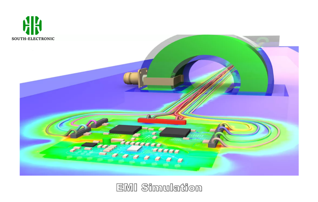
How to Avoid Common EMI Issues in Multilayer PCB Stack-ups?
EMI problems often trace back to poor return current paths and inadequate shielding in the stack-up.
Implement contiguous ground planes, minimize split planes, and use buried capacitance layers. Maintain <20mil spacing between high-speed signals and reference planes while controlling dielectric thickness tolerances.
)
EMI Prevention Checklist
Essential stack-up features for EMI control:
| Technique | Implementation | Effectiveness |
|---|---|---|
| Ground Plane Shielding[^7] | Place ground layers adjacent to signal | Reduces EMI by 60-70% |
| Differential Pair Routing[^8] | Tight coupling with reference plane | Lowers Crosstalk 45% |
| Edge Guard Traces | 50mil ground traces along board edges | Cuts Edge EMI 30dB |
| Decoupling Capacitor Placement | Within 100mil of IC power pins | Suppresses Noise 50% |
When designing a 12-layer telecom PCB, adding dedicated shielding layers between analog and digital sections dropped radiated emissions from 52dBµV/m to 38dBµV/m – meeting FCC Class B requirements with margin.
Conclusion
Successful multilayer stack-ups balance electrical performance, thermal management and manufacturing reality through calculated layer choices, material science, and EMI-aware geometric planning.
[^1]: Explore this resource to understand the essential techniques and strategies for effective multilayer PCB stack-up construction, ensuring optimal performance and reliability.
[^2]: This link will provide insights into EMI mitigation strategies, crucial for maintaining signal integrity and reducing interference in PCB designs.
[^3]: Discover the factors that affect layer count in PCB design, helping you make informed decisions for your projects and avoid costly mistakes.
[^4]: Understanding Dk stability is crucial for ensuring signal integrity in high-speed applications. Explore this link to learn more.
[^5]: Rogers 4350B is a key material for high-speed signals. Learn about its unique properties and why it’s preferred in PCB design.
[^6]: High-thermal-conductivity substrates are vital for power layers in PCBs. Discover their benefits and applications through this resource.
[^7]: Ground plane shielding is crucial for reducing EMI. This resource will provide you with effective strategies and techniques.
[^8]: Learn about differential pair routing to enhance your PCB designs and minimize crosstalk issues effectively.

