

Ever frowned at your circuit board, wondering why that IC overheats? You pick the wrong package, risking burnt chips and failed devices. This causes costly redesigns and shipping delays. My method prevents those headaches.
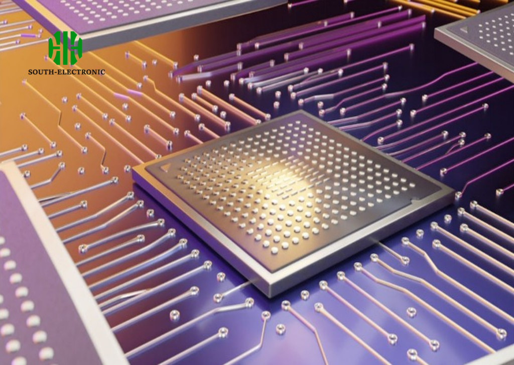
Select IC packages[^1] by balancing four factors: signal speed needs[^2], heat dissipation limits[^3], board space availability, and manufacturing costs. BGA[^4] suits high-power/high-speed chips, QFN[^5] fits compact designs, and SOT[^6] works for simple circuits. Always check datasheets first.
Choosing blindly leads to melted components or botched production runs. Stick around to understand package tradeoffs – your next product deserves reliable performance.
How many types of IC packages are there?
Picture laptop factory chaos: technicians juggling tiny chips. Using the wrong SMD package halts production. Undersized parts cause fitting errors. Oversized ones waste precious PCB space. Recognizing common types solves this.
Main surface-mount packages include QFP (high pin counts), BGA (heat-intensive chips), QFN (compact modules), and SOT (basic components). Over 20 variants exist, but these cover 90% of modern electronics needs.

Core SMD Categories Explained
We organize packages by pin arrangement and size:
| Package Type | Pins | Typical Use Case | Size Factor |
|---|---|---|---|
| BGA | 100-1000+ | Processors, FPGAs | Large footprint |
| QFP | 32-256 | Microcontrollers | Medium |
| QFN | 8-100 | Power management ICs | Compact |
| SOT | 2-8 | Transistors, diodes | Ultra-small |
Pin count determines package choice – complex processors need BGA’s dense grid. Small ICs like voltage regulators fit tiny QFN bodies. Simple components use gull-wing SOT cases. Ball grid arrays (BGA) dominate high-performance applications but require precise soldering. Quad flat packages (QFP) offer reliable mid-tier solutions. Quad flat no-lead (QFN) saves space with thermal pads underneath. Board thickness limitations influence choices too: thin gadgets often demand low-profile QFNs.
How does IC package choice impact cost, performance, and reliability of your product?
Billions evaporate from chip shortages annually. Wrong packaging multiplies expenses. Cheap packages crack under vibration. Oversized ones inflate PCB costs. A strategic pick optimizes value and lifespan.
Package directly affects final product: cost scales with material size, speed compatibility defines performance, and build quality influences failure rates. QFN cuts assembly expenses while BGA enhances heat endurance for demanding tasks.

The Triple Constraint Breakdown
Every package imposes tradeoffs:
| Factor | Cheapest (SOT) | Balanced (QFP) | High-End (BGA) |
|---|---|---|---|
| Unit Cost | $0.01-0.10 | $0.15-0.80 | $1.00-5.00+ |
| Max Speed | <100 MHz | 100-500 MHz | 1+ GHz |
| Thermal Tolerance | Low | Medium | High |
| Board Fatigue | Moderate risk | Low risk | Very low risk |
Reliability links tightly to structural design. Thin QFPs may bend during thermal cycling while BGAs withstand stress via solder balls. Performance depends on lead length – short BGA routes support fast signals. Cost analysis goes beyond components: QFN requires cheaper pick-and-place tools than BGA. Power budgets matter too – inadequate cooling transforms cost savings into field failures. Daily smartphone drops? Robust BGAs survive better than thin-leaded models.
What's new in advanced IC packaging beyond BGA?
Traditional packages constrain modern AI chips. Standard BGAs hit density ceilings. Overheating throttles 5G devices. Thin phones reject bulky solutions. Next-gen approaches like chiplets and silicon bridges overcome these walls.
Innovations include 2.5D interposers for stacking dies, fine-pitch micro-BGAs, and fan-out wafer-level packaging[^7] (FOWLP). These boost speed by 40% while shrinking footprints. TSMC's CoWoS and Intel's EMIB lead this evolution.

Revolutionizing Chip Integration
New methods focus on energy efficiency and space reduction:
| Technology | Key Improvement | Best For | Limitation |
|---|---|---|---|
| 2.5D with TSVs | Vertical connection stacking | High-bandwidth memory | Complex manufacturing |
| Panel-Level FOWLP | Larger production panels | Cost-sensitive applications | Yield challenges |
| Hybrid Bonding | Sub-micron interconnects | AI accelerators | Extreme cleanliness |
Chiplet designs split complex systems – process blocks get optimized packages then networked organically. Fan-out methods eliminate substrates by embedding dice in epoxy. Micro-BGAs offer 0.3mm pitches versus standard 0.8mm. Thermal budgets improve with direct liquid cooling channels. Challenges remain: microscopic 5µm traces demand perfection, and testing multi-die assemblies complicates quality control. These innovations prove crucial for wearables and edge computing – devices needing crammed circuitry.
Conclusion
Picking IC packages demands evaluating signal needs, heat limits, space constraints, and costs. Advanced options like FOWLP address modern challenges, but classic packages still dominate everyday designs.
[^1]: Explore this link to understand the various IC packages and their applications in modern electronics.
[^2]: Learn how signal speed requirements influence the choice of IC packages for optimal performance.
[^3]: Discover the importance of heat dissipation in IC package selection to prevent overheating.
[^4]: Explore the benefits of BGA packages for high-performance applications and their thermal management.
[^5]: Learn about QFN packaging and how it fits into compact electronic designs.
[^6]: Discover the common uses of SOT packages for basic components in electronic circuits.
[^7]: Learn about fan-out wafer-level packaging and how it revolutionizes chip integration.

