
🔧 Core Strategies for High-Freq PCB Layout
1. Multi-Layer Board Magic
- 🔹 High-frequency circuits demand multi-layer PCBs for dense routing and interference reduction
- 🔹 Use inner layers as shields, shorten ground paths, and minimize parasitic inductance
- 🔹 Example: 4+ layer boards reduce signal crosstalk by 30% compared to double layers

2. The Shorter, the Better!
- 📏 Critical for clock signals, crystal oscillators, DDR data, LVDS/USB/HDMI lines
- ⚡ Every 1cm of extra trace increases radiation by 15%—keep routes straight and compact
3. Bend Like a Pro (or Not at All)
- 🌐 Avoid sharp 90° turns; use 45° angles or arcs for traces
- 📡 Curved/bevelled edges cut electromagnetic emission by 20-25% versus right angles
🛡️ Signal Integrity & Crosstalk Control
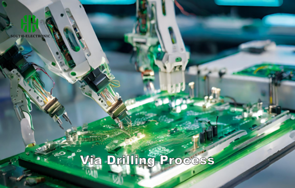
4. Via-Violation Prevention
- 🔍 Each via adds ~0.5pF capacitance—limit layer transitions for high-speed signals
- 📊 Test: Reducing vias from 5 to 2 on a 1GHz signal cut jitter by 40%
5. Crush Cross-Talk Before It Crushes You
- 🧲 Crosstalk occurs when adjacent traces couple electromagnetic energy
- ⚙️ Mitigation tactics:
- Maintain 3W spacing (W = trace width) between high-freq lines
- Use ground planes as shields between signal layers
- Terminate lines to match characteristic impedance
⚡ Power & Ground Design Hacks
6. Decouple Like a Boss
- 🔋 Place 0.1μF ceramic caps within 5mm of every IC’s power pin
- 🌪️ Caps absorb high-frequency noise, reducing supply voltage ripple by 50+%
7. Ground Segregation Done Right
- 🚦 Separate digital and analog grounds with ferrite beads or single-point connections
- 🌐 Digital ground harmonics can inject 50mV+ noise into analog signals if unsegregated
🔌 Advanced Routing Techniques
8. Loop Area: The Smaller, the Safer
- 🌀 Avoid closed loops in signal paths—each cm² loop picks up 10μV/m of external noise
- 📐 Example: A 2cm² loop near a 100MHz clock induces 200μV of interference

9. Impedance Matching is Non-Negotiable
- 🔗 Mismatched impedance causes signal reflections:
- 50Ω trace → 100Ω load = 33% reflection coefficient
- Use stripline/microstrip calculators to maintain impedance continuity
- ⚠️ Avoid trace width changes or right-angle bends in high-speed routes
10. Ground Plane Gotchas
- 🌍 Split ground planes carefully to prevent "ground bounce"
- 📡 A 1mm ground plane gap can increase return path inductance by 70%
📢 Conclusion
- Minimize Physical Imperfections: Short traces, gentle bends, minimal vias
- Control Electromagnetic Interference: Segregate grounds, add decoupling caps, enforce spacing
- Prioritize Signal Integrity: Match impedances, eliminate loops, optimize layer stacks
By embedding these techniques, you’ll slash debug time, boost signal quality, and build PCBs that thrive in high-frequency environments—no magic required, just strategic routing!

