

Incorrect pad size, alignment, or placement on a PCB can cause issues with component electrical performance and manufacturability. PCB pad design is like the foundation of a house: if the foundation isn’t laid properly, how stable is the house? Similarly, if the PCB pad design is faulty, how reliable is the board?
What are pads in PCB design?
Pads are exposed metal areas on the board that connect the circuitry on the die to the pins on the chip package.

Problems Caused by Incorrect Pad Size in PCBs
The size, shape, and placement of pads in a PCB package directly impact the manufacturability of the board. Using incorrectly sized or positioned pads can lead to various issues during the soldering process of PCB assembly, including the following:
- Floating Components
If a surface mount component is placed on a pad that is too large or incorrectly spaced, the component may float out of position during reflow soldering. This can cause solder bridging to other metals and lead to inadequate component spacing for thermal cooling, rework, and PCB testing.
- Incomplete Solder Joints
Pads that are too small or too closely spaced may not have enough space to form an adequate solder fillet. This can result in a poor solder connection or no solder joint at all.
- Solder Bridging
Surface mount pads that are too large can cause the part to float, which can lead to solder bridging. This occurs when solder flows over a pad or metal feature on another net and creates a direct short. Solder bridging can also occur if the correct solder mask and solder paste features are not designed into the pad shape in the CAD tool.
- Tombstone
Two small, fixed SMT parts, such as resistors and capacitors, can experience soldering issues if their pads are unequal in size. One pad will heat faster than the other, and the molten solder will pull the part upwards and away from the other pad, causing it to stick like a tombstone.

- Solder Wicking
Through-hole pads can also experience difficulties if not constructed correctly. If a drill size that is too large is used for the component lead entering the hole, solder may wick through the hole before a good connection is formed. On the other hand, a drill bit that is too small can make inserting component leads difficult and slow assembly.
- Through-hole Breaks
Through-hole pads must have a solid annular ring to ensure solderability. This ring is the metal between the hole wall and the outer perimeter of the pad. The annular ring is designed to be large enough to allow the drill bit to deviate from the hole center as intended. However, if the pad is too small, some breakage in the annular ring may occur, and excessive breakage can lead to improper soldering or damaged and incomplete circuits.
If the pad size is too small for the drill hole used, the drill bit may wobble slightly and break away from the pad shape during normal drilling operations.

- Shorts to Other Metals
A pad that is too small can place surface traces too close to the component being soldered to it, creating a potential metal shorting area. On the other hand, a pad that is too large can restrict the routing of traces between them, making board routing more difficult.
Classification of Pad Design in PCBs
- Surface Mount Pads
1.1. Pads used to mount surface mount components are called surface mount pads. These pads have the following characteristics: A pad showing copper area. This can be rectangular, round, square, or other shapes.
1.2. Solder Mask
1.3. Solder Paste
1.4. Pad Numbering (the number of pads present on a component)
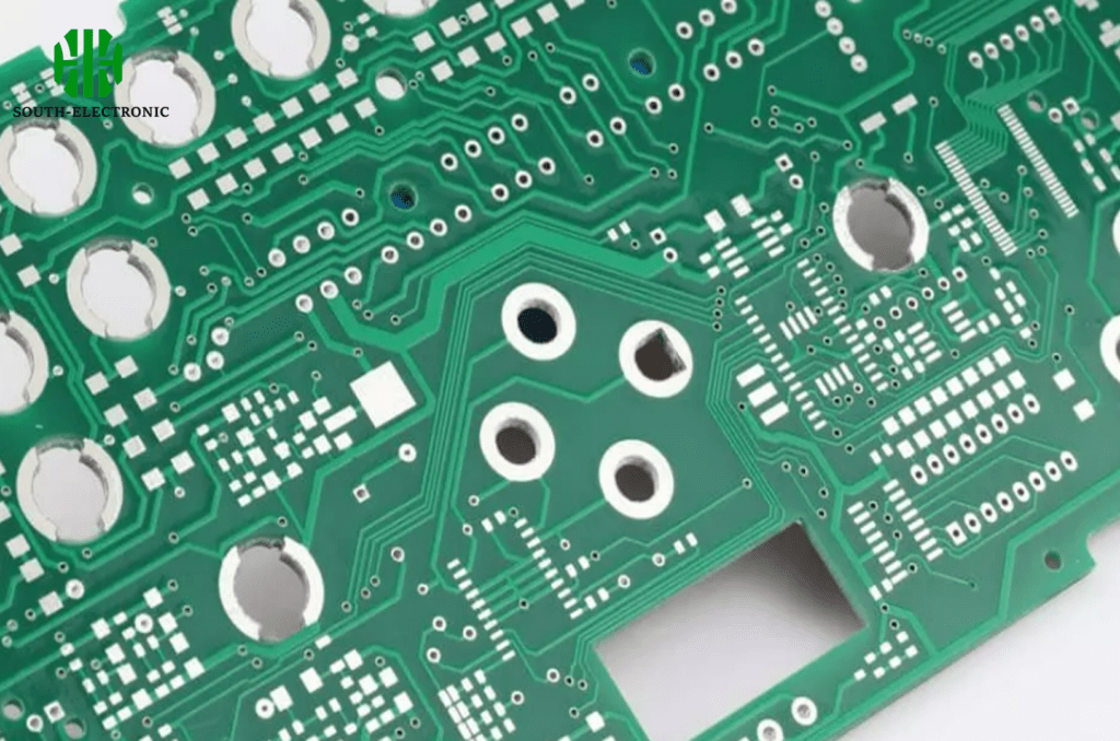
- Through-Hole Pads
Through-hole pads are pads used to mount through-hole components. There are two types:
2.1. Plated Through-Hole (PTH)
A PTH is a pad with a through-hole. The hole walls are plated with copper and sometimes with solder or another protective coating. The hole plating is done using an electrolytic process, and the plating provides an electrical connection between different layers of the circuit board.
2.2. Non-Plated Through-Hole (NPTH)
NPTH pads are pads with no plating in the hole. These pads are primarily used in single-sided boards or for mounting the PCB in an enclosure, where screws are installed. Typically, unplated holes have no copper in the area surrounding the hole (similar to a board edge gap). This is done to prevent shorts between the copper layer and the component being placed.
The different parts of a through-hole pad are often referred to as the pad stack and include:
- Top pad
- Bottom pad
- Inner pad
- Drill bit
- Annular ring
- Pin size
- Special Features of BGA Pads
3.1. SMD Pads vs. NSMD Pads
Proper pad design is critical to ensuring the manufacturability of BGA components. There are essentially two types of BGA pads—solder mask defined pads (SMD) and non-solder mask defined pads (NSMD).
3.2. Solder mask defined (SMD) BGA pads
SMD pads are defined by solder mask holes applied to the BGA pad. These pads have solder mask holes that make the mask opening smaller than the diameter of the pad they cover. This is done to reduce the size of the copper pad to which the component is soldered.
The following figure shows how to specify that the solder mask covers a portion of the underlying copper pad.
This offers two advantages. First, the overlapping mask helps prevent the pad from lifting from the board due to mechanical or thermal stress. Second, the openings in the mask create a channel for each BGA solder ball to align with it as the part passes through the soldering process.
The copper layer of SMD BGA pads typically has the same diameter as the pads on the BGA. To create SMD coverage, a 20% reduction is traditionally used.
3.3. Non-Soldermask Defined BGA Pads (NSMD)
NSMD pads differ from SMD pads in that the solder mask is defined not to contact the copper pad. A mask is created to create a gap between the pad edge and the solder mask.
Here, the copper pad size is defined by the copper pad diameter rather than the mask layer.
NSMD pads can be smaller than the solder ball diameter, with the pad size reduction being 20%
How to Get PCB Pad Design Dimensions?
The following methods can be used to determine the correct size and shape for the PCB pads and component footprints you will use.
- Industry Standards
Over the years, the PCB design industry has established standards for various aspects of board layout, including recommended pad and land pattern sizes. IPC-7351 is one such standard, but there are others.
- Pad and Land Pattern Generators
Today’s electronic design automation (EDA) tools include pad and land pattern generators, also known as library wizards. These software features are often integrated with IPC standards and will automatically generate the required pad shapes and sizes for a component.
- Component Supplier Datasheets
Every PCB component manufacturer publishes a datasheet for the parts they offer. In addition to the electrical and physical specifications in these datasheets, they often include recommended PCB layout land patterns.
- Pad and Land Pattern Calculators
Engineers and other users can find a variety of pad and land pattern calculators online.

- Company Standards
Many companies have their own pad and land pattern standards that they prefer to adhere to when designing circuit boards. These footprints are often a combination of industry standards and vendor specifications tailored to specific PCB manufacturers.
- PCB Design CAD Vendor Libraries
EDA tools also offer pre-made pad libraries and land patterns that can be downloaded and used. These are available to users who have purchased a license to use the design tool.
- PCB Manufacturers
Individual PCB contract manufacturers may also have preferred PCB pad sizes and land patterns that they prefer you to adhere to. They should be able to provide pad sizes and shapes that best suit their own manufacturing processes.
- Third-Party Library Providers
There are also several online PCB library providers that have already constructed pads and land patterns and offer them for use.
However, the size and shape of the pads used in a PCB aren’t the only specifications that should be regulated by standards; spacing for precise component placement is also important. If components are placed too close together on the board, you may experience the same solder bridging problem as when pads are incorrectly sized.
PCB Design Pad Shape and Size Standards (For Reference Only)
-
The minimum single-side diameter of all pads should be no less than 0.25mm, and the maximum overall pad diameter should be no more than three times the component aperture diameter.
-
The distance between pad edges should be at least 0.4mm.
-
For densely spaced layouts, oval and rectangular round pads are recommended. The minimum diameter or width of single-sided pads is 1.6mm; double-sided weak circuit pads only require a 0.5mm aperture. If the pad is too large, it can easily cause unnecessary joint soldering. Pads with an aperture diameter exceeding 1.2mm or a pad diameter exceeding 3.0mm should be designed as diamond or plum blossom pads.
-
For plug-in components, to prevent copper foil damage during soldering, single-sided connection pads should be fully covered with copper foil; however, the minimum requirement for double-sided boards is to compensate for teardrops.
-
All machine parts must be designed with drip pads along the bend direction to ensure full solder joints at the bend.
-
For large copper pads, use daisy-shaped pads instead of dummy pads. If the PCB has large ground and power trace areas (over 500 mm²), these should be partially open-circuited or designed with a grid fill.
PCB Pad Design and Manufacturing Process Requirements (for reference only)

-
Test components should be placed where the ends of surface mount components are not connected to plug-in components. The diameter of the test point should be equal to or greater than 1.8 mm to facilitate testing with an in-circuit tester.
-
For tightly spaced IC pads that do not connect to plug-in pads, a test pad should be added. For surface mount ICs, test points should not be placed within the silkscreen. The diameter of the test point should be equal to or greater than 1.8 mm to facilitate testing with an in-circuit tester.
-
If the pad spacing is less than 0.4 mm, white solder paste must be applied to reduce over-peak soldering.
-
The tips and ends of SMD components should be soldered with lead-tin. The recommended soldering width is 0.5mm, and the length is generally 2-3mm.
-
If hand-soldered components are used on a single-sided board, the solder bath should be opened. The direction should be opposite to the soldering direction. The hole width should be 0.3mm to 1.0mm.
-
The spacing and size of the conductive adhesive buttons should be consistent with the actual size of the conductive adhesive buttons. The PCB board to which it is connected should be designed with gold fingers and the corresponding gold plating thickness should be specified.


