

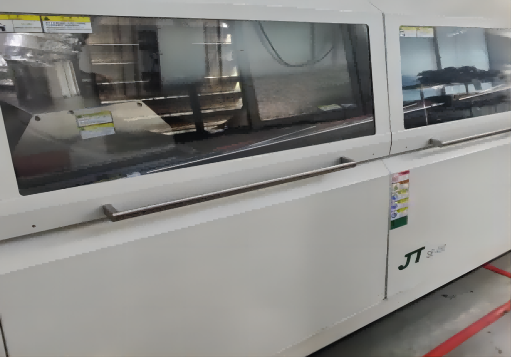
1. Hot Plate, Push Plate Conduction Reflow
This type of reflow oven relies on a heat source under a conveyor belt or push plate, heating the components on the substrate through heat conduction. It is used for single-sided assembly of thick-film circuits on ceramic (AI203) substrates. The ceramic substrate can only receive sufficient heat when placed on the conveyor belt. Its structure is simple and its price is low. Some thick-film circuit manufacturers in my country introduced this type of equipment in the early 1980s.
2. Infrared Radiation Reflow
This type of reflow oven is also mostly conveyor-type, but the conveyor belt only supports and transports the substrate. Its heating method relies primarily on infrared radiation heating. The temperature within the furnace is more uniform than the previous type, and the mesh is larger, making it suitable for reflow heating of double-sided assembled substrates. This type of reflow oven can be considered the basic type of reflow oven. It is widely used in my country and is relatively affordable.
3. Infrared Heating Air Reflow Oven
This type of reflow oven is based on an IR oven and adds hot air to make the temperature inside the oven more uniform. When using infrared radiation heating alone, people have found that in the same heating environment, different materials and colors absorb different amounts of heat, that is, the O value in formula (1) is different, and thus the temperature rise T is also different. For example, the package of SMDs such as ICs is black aldehyde or epoxy, while the leads are white metal. When heated alone, the temperature of the leads is lower than that of the black SMD body. Adding hot air can make the temperature more uniform and overcome the difference in heat absorption and poor shadowing. IR+hot air reflow ovens were once widely used internationally.
4. Helium Reflow Oven
With the increase in assembly density and the emergence of fine pitch assembly technology, nitrogen-filled reflow oven processes and equipment have been developed, which have improved the quality and yield of reflow ovens and have become the development direction of reflow ovens. Nitrogen reflow offers the following advantages:
- Prevents and reduces oxidation
- Improves solder wetting and accelerates wetting
- Reduces solder balls, avoids bridging, and achieves superior solder quality
Higher solder quality is particularly important because it allows the use of tin with lower-activity flux, which also improves solder joint performance and reduces substrate discoloration. However, the downside is a significant increase in cost, which increases with the amount of nitrogen used. The difference in nitrogen requirements when requiring a furnace oxygen level of 1000ppm versus 50ppm is significant. Current solder paste manufacturers are developing no-clean soldering methods that can achieve excellent joints in higher oxygen atmospheres, thereby reducing nitrogen consumption. A cost-benefit analysis must be conducted for the introduction of nitrogen into reflow. Benefits include product yield, improved quality, and reduced rework or repair costs. A thorough analysis often reveals that nitrogen introduction does not increase final costs but rather provides significant benefits. Most ovens currently in use are forced hot air circulation types, making it challenging to control ammonia consumption in these ovens.
5. Double-Sided Reflow
Double-sided PCBs are already quite common and are becoming increasingly popular. Their popularity stems primarily from the flexibility they offer designers, enabling them to design smaller, more compact, and lower-cost products. To date, double-sided PCBs have typically been reflowed on the top (component side) and then wave soldered on the bottom (pin side). While the current trend is toward double-sided reflow, this process still presents some challenges. Components on the bottom of a large board can fall off during the second reflow process, or the bottom solder joints can partially melt, causing solder joint reliability issues.
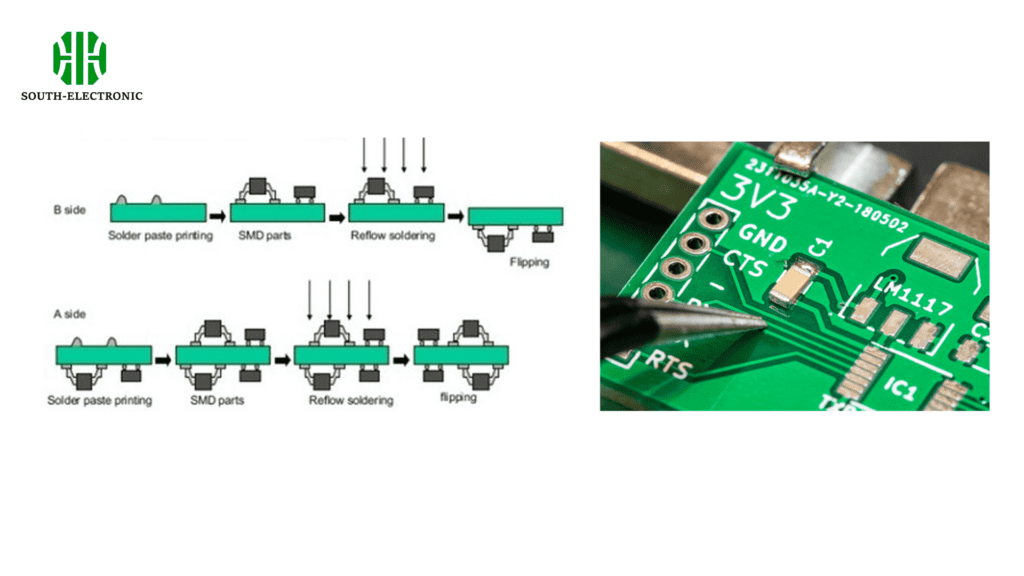
Several methods have been developed to achieve double-sided reflow:
One approach involves using glue to secure components on the first side. This secures the components in place when the board is flipped over for a second reflow. This method is commonly used, but requires additional equipment and steps, which increases costs.
The second method involves using solder alloys with different melting points: a higher-melting-point alloy for the first side and a lower-melting-point alloy for the second side. The problem with this approach is that the choice of lower-melting-point alloy may be limited by the operating temperature of the final product, while higher-melting-point alloys inevitably require higher reflow temperatures, potentially damaging both the components and the PCB itself. For most components, the surface tension of the molten solder at the weld point is sufficient to hold the component on the bottom, forming a highly reliable solder joint. The ratio of component weight to lead area is a key metric for successful soldering; a typical design standard of 30g/in² is used.
The third method involves blowing cold air through the bottom of the furnace to maintain the solder joint temperature below the melting point during the second reflow. However, a potential problem is the internal stress caused by the temperature difference between the top and bottom surfaces, requiring effective methods and processes to eliminate this stress and improve reliability. These process challenges are not simple, but they are being successfully addressed. Undoubtedly, double-sided boards will continue to grow significantly in number and complexity over the next few years.
6. Through-Hole Reflow
Through-hole reflow, sometimes also called component-sorting reflow, is gaining popularity. It eliminates the wave soldering process and becomes a key step in PCB assembly. One of its key advantages is that it leverages the advantages of surface mount manufacturing while utilizing through-hole soldering technology to achieve superior mechanical connection strength. However, the flatness of larger PCBs may not allow all surface mount component pins to contact the solder pads. Furthermore, even if contact is achieved, the mechanical strength provided is often insufficient, making it prone to detachment during product operation and becoming a point of failure.
While through-hole reflow offers significant benefits, it does have several drawbacks in practical applications. The high volume of solder paste increases the risk of machine contamination due to flux evaporation and cooling, necessitating an effective flux residue removal system. Another issue is that many connectors are not designed to withstand reflow soldering temperatures. Early direct infrared heating ovens are no longer suitable, as they lack the heat transfer efficiency to handle the complex geometries of through-hole connectors placed on the same PCB as standard surface-mount components. Only large-capacity forced convection ovens with high heat transfer are practical and proven to be effective for through-hole reflow. The remaining challenge is ensuring a suitable reflow profile for the solder paste in the through-holes and the component leads. With improvements in processes and components, through-hole reflow will become increasingly popular.
The advantages of through-hole reflow soldering technology include:
-
High reliability and excellent soldering quality, with a defect rate (DPPM) below 20.
-
Fewer solder joint defects such as cold solder joints and bridging, reducing the amount of board repair work.
-
Clean PCB surfaces with a significantly better appearance than wave soldering.
-
Simplified process. By eliminating the dispensing (or printing) of surface mount adhesive, wave soldering, and cleaning steps, both operation and management are simplified. 5. Reduce costs and increase efficiency.
7. Lead-free reflow soldering
For environmental reasons, the use of lead will be strictly restricted in the 21st century. Although lead usage in the electronics industry is minimal, less than 1% of total usage, it is still banned and will be phased out over the next few years. Reliable and economical lead-free solders are currently being developed. The various alternatives currently available generally have melting points approximately 40°C higher than tin-lead alloys, which means reflow soldering must be performed at higher temperatures. Nitrogen protection can partially mitigate the increased oxidation and damage to the PCB itself caused by the increased temperature. However, the industry will likely have to go through a painful learning period to resolve the issues it encounters. The time saved by quickly adopting this process is already limited. Many current ovens are designed for operating temperatures no higher than 3000°C. Lead-free solders or non-eutectic solders (used for BGAs, double-sided boards, etc.) require higher oven temperatures. These new processes typically require temperatures in the reflow zone of 3500°C to 4000°C. Oven designs must be modified to meet these requirements, and heat-sensitive components in the machine must be modified or measures must be taken to prevent heat transfer to these components.
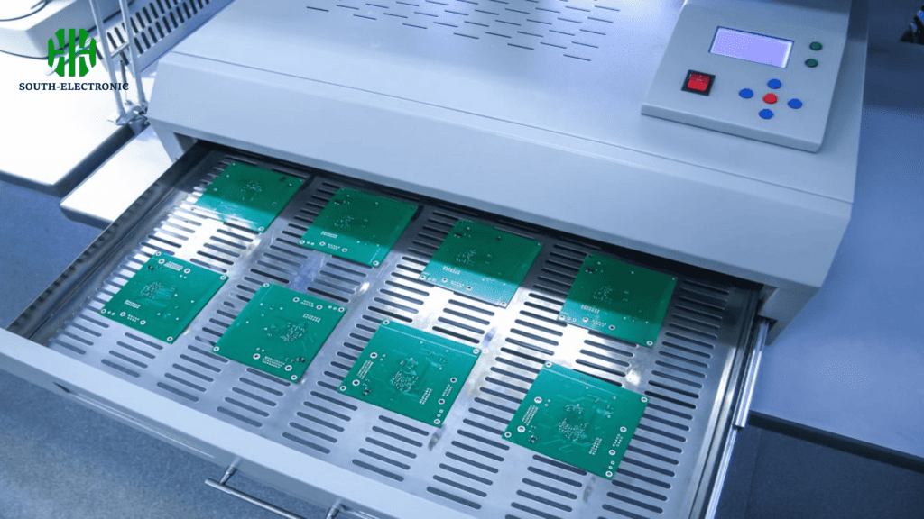
8. Continuous Flex Board Reflow
Specialized ovens have been developed to process continuous flex boards with SMT components mounted on them. The main difference from conventional reflow ovens is that these ovens require a specialized track to transport the flex boards. Of course, these ovens also need to be able to handle continuous boards. For discrete PCBs, the flow rate within the furnace is independent of the conditions of the preceding stations. However, for continuous rolls of flexible PCBs, the PCB runs continuously throughout the entire production line. Any specific issue in the line could cause a pause, forcing the entire line to stop. This presents a unique problem: the section stopped in the furnace could be damaged by overheating. Therefore, such furnaces must be able to adapt to random pauses, continue processing that section of PCB, and return to normal operation when the entire line resumes continuous operation.
9. Vertical Vacuum Reflow Oven

Market demand for smaller sizes has led to the widespread use of CSPs (such as flip chips), which offer a smaller footprint and higher signal transmission rates after component placement. Filling or potting is used to strengthen the solder joint structure to withstand the stress caused by the mismatch in thermal expansion coefficients between the silicon wafer and the PCB material. Typically, a drop-on or grommet-fill method is used to seal the wafer with adhesive. Many of these encapsulants require very long cure times, making them impractical for in-line production ovens. Batch ovens are typically used, but vertical ovens have proven successful in performing the curing process, and their temperature profiles are simpler than those of conventional reflow ovens. Vertical ovens use a PCB conveyor system to act as a buffer/accumulation area, extending the time the PCBs spend in a small oven footprint.
Almost all of these encapsulants require very long cure times, making in-line continuous production ovens impractical. Batch ovens are commonly used, but vertical oven technology is becoming increasingly sophisticated, particularly when the heating profile is simpler than that of a reflow oven. Vertical ovens use a vertical lift conveyor system as a "buffer and accumulator," through which each PCB must pass through the process. This results in a sufficiently long cure time while reducing the footprint.

