
Gerber files for PCBs are the most widely accepted design file format for manufacturing and assembling printed circuit boards (PCBs). They ensure an efficient manufacturing process by standardizing the transfer of design data between engineers and PCB manufacturers. Once a circuit design is finalized and an order is placed, the contract manufacturer will require the design files to accurately fabricate the PCB.
Errors in the provided data inevitably lead to board defects, additional costs, and time delays. To prevent these consequences, Gerber files play a crucial role in PCB manufacturing.
What are Gerber files? What information do they contain?
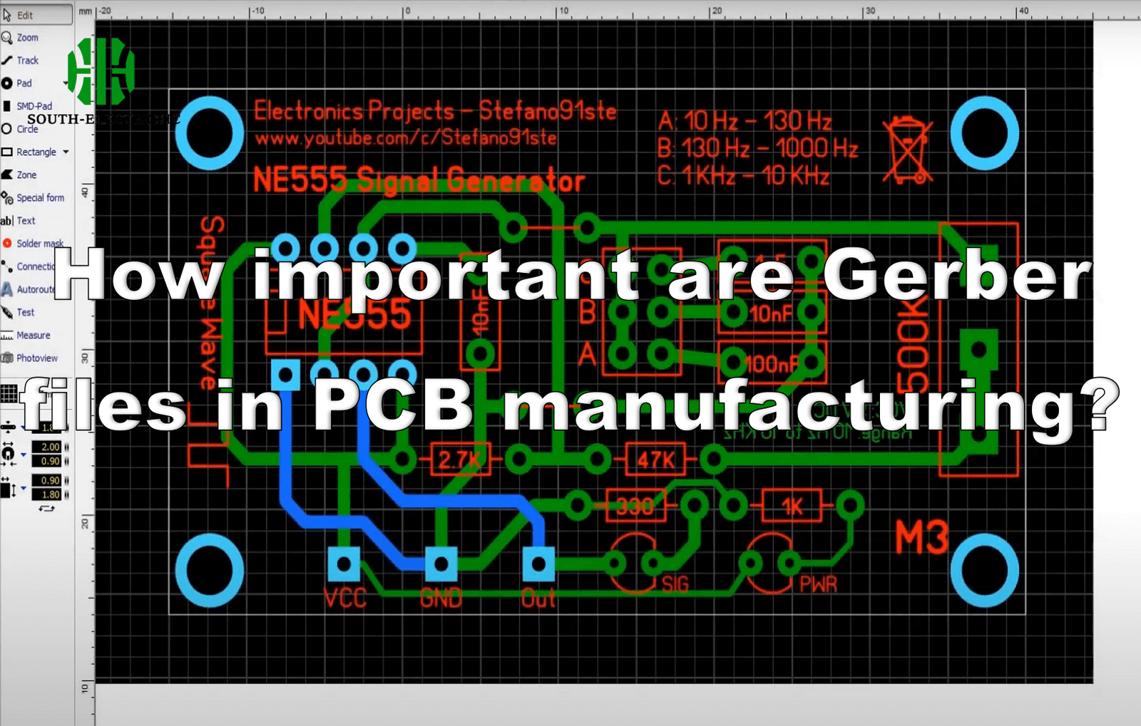
Gerber files are a series of ASCII vector-formatted files that define PCB design specifications. Generated using electronic design automation (EDA) or computer-aided design (CAD) tools, they provide information such as board configuration parameters, aperture descriptions, XY coordinate locations, and drawing instructions. Configuration details include the size and shape of the PCB to be manufactured.
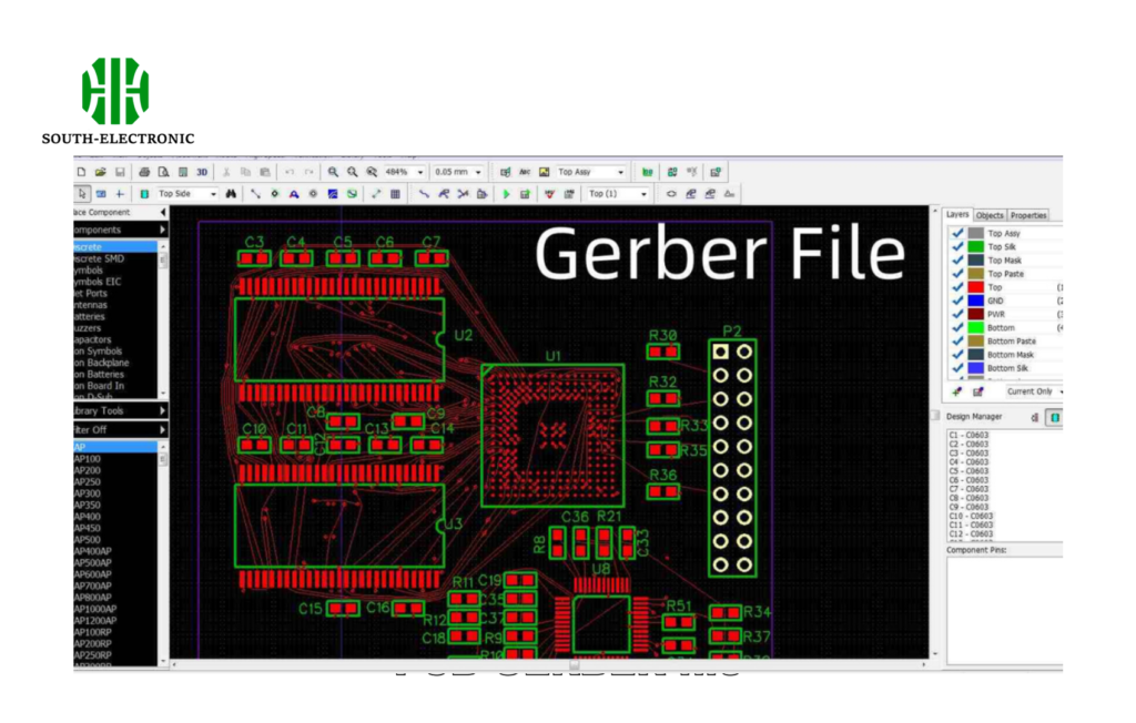
Each layer of the board is recorded in a separate file, defining components such as copper traces, pads, vias, solder mask, silkscreen, and logos. A Gerber file specifies the XY coordinate location of each geometric shape and uses instructions to draw these shapes on the physical board.
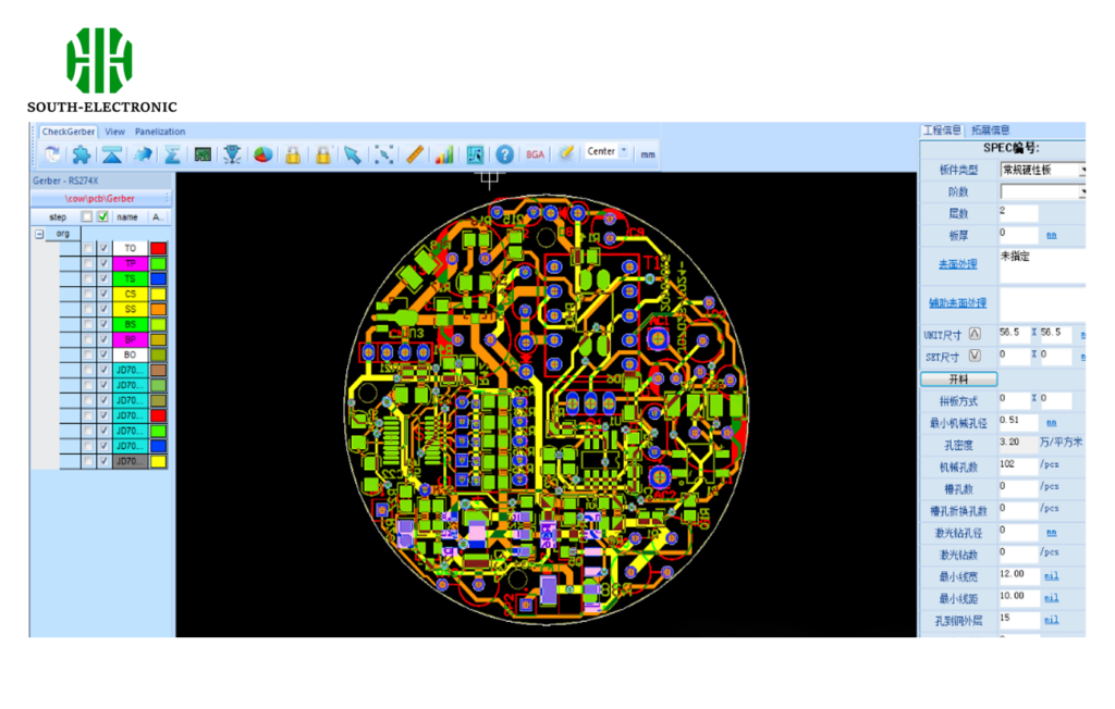
The basic components of a Gerber file include: board dimensions, outline, top assembly, top silkscreen, top solder mask, top paste, top copper, internal signals, inner layers, bottom copper, bottom paste, bottom solder mask, bottom silkscreen, bottom assembly, and manufacturing information (providing information such as stackup, drill details, and cutouts).
Gerber files generated by computer-aided manufacturing (CAM) tools have user-selectable extensions, typically using a naming scheme such as ".TOP" for top layer, ".BOT" for bottom layer, and ".drl" for drill data.
The Importance of Gerber Files in PCB Manufacturing
PCB designers must create Gerber files using EDA tools compatible with the PCB manufacturer’s systems. Incompatible formats or tool versions can cause delays in the manufacturing process. The primary goal of Gerber files is to deliver reliable PCB orders within the expected timeframe. Using Gerber files in PCB manufacturing offers many benefits, including:

Gerber files provide intricate design details, helping PCB manufacturers build high-quality boards. Contract manufacturers rely on these files to ensure the accuracy of board dimensions, pad locations, trace widths, and silkscreen legends. The accurate data provided by Gerber files significantly reduces potential manufacturing errors.
They are compatible with a wide range of CAM tools used by PCB manufacturers. Gerber files can be easily exported from most EDA tools, ensuring a smooth transition from design to production in the PCB development cycle. Furthermore, the flexible data format allows contract manufacturers to utilize various manufacturing and assembly techniques, supporting advanced technologies.
The standardized format of Gerber files is crucial for establishing a flawless PCB manufacturing process. These easy-to-read files are convenient for design engineers, layout specialists, and assembly line technicians to use, reducing confusion and minimizing rework throughout the manufacturing process.
Contract manufacturers often use Gerber files for Design for Manufacturability (DFM) checks and assessing production yield. Similarly, these files are used to create jigs for board inspection and testing, aiding quality control in PCB production.
Gerber File Versions and Other Output Formats
The size and complexity of the board determine the type and number of Gerber files generated. While the data structures of different Gerber file formats vary, they are all used to create templates for PCB manufacturing.
RS274-D is the standard Gerber file format, a numerically controlled format consisting of XY coordinates and drawing codes, designated by the ".gbr" extension. It was initially very popular. However, this format required manual assignment of aperture codes to generate accurate Gerber files, leading to the development of the extended Gerber format.
RS274-X is a revised version, with the ".gbx" extension. This ASCII format combines the four main components of Gerber information (configuration parameters, aperture diagram, XY coordinates, and drawing instructions) into a single file. In this format, aperture positions are automatically updated.
Gerber X2 is the latest file version, containing additional data such as layer stackup details, via and pad attributes, and impedance-controlled traces. It supports extensions such as ".top" and ".bot". This format is backwards compatible with RS274-X but includes a wealth of manufacturing data, significantly reducing file errors and data ambiguity.
Open Database (ODB++) is another data exchange format that contains all the information needed to define PCB layers in a single file. This allows designers to capture all the data needed for design-for-manufacturing (DFM) checks, such as board stackup, bill of materials, dimensions, and drill details. It is supported by major CAM and DFM tools.
IPC-2581 is the latest standard for organizing and exchanging PCB data from CAD to CAM systems during the manufacturing and assembly process. It is an open standard for data transmission without manual intervention. XML-based files are used to provide all manufacturing data to CAM systems, allowing design data to be directly extracted without requiring CAM interpretation.
Gerber files are a widely used data transmission format in the PCB manufacturing industry, supporting high-volume production of PCB products. The latest version, Gerber X2, has become a popular format among manufacturers for delivering high-performance and reliable PCBs. These Gerber files reduce manufacturing errors, improve efficiency, and accelerate time to market.

