

Testing circuits shouldn’t break the bank. Expensive solutions frustrate designers. Low-cost test points solve this pain economically. Let me show you smart alternatives!
Low-cost PCB test points are designated access locations like copper pads, vias, or metal loops enabling circuit probing without component removal. They provide affordable manufacturing testing through simple design adaptations like reusing existing features or phosphorus-bronze wires.

Now that you know the basics, let’s explore key questions about implementing these solutions efficiently.
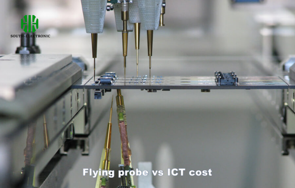
Flying Probe vs. ICT Testing: Which Saves More for Low-Volume PCB Orders?
Choosing test methods feels overwhelming. Wrong picks drain budgets fast. Compare these approaches before ordering!
Flying probe testing costs less for prototypes and small batches under 500 units—no fixture fees! ICT (In-Circuit Testing) suits mass production due to faster per-unit times despite higher initial setup.
Breaking Down Cost and Application Factors
Several elements determine which method saves money:
| Factor | Flying Probe | ICT |
|---|---|---|
| Setup Cost | None ($0 fixtures) | High ($500-$10k) |
| Speed per Board | Slow (minutes) | Fast (seconds) |
| Ideal Batch Size | Under 500 units | Over 500 units |
| Flexibility | Handles design changes | Requires new fixtures |
| Fault Detection | Good for opens/shorts | Excellent for components |
For small runs under 500 boards, flying probe consistently wins on cost. Why pay thousands for fixtures you’ll never reuse? Prototypes change constantly—flexible flying probes adjust instantly. ICT wins on assembly-line speed but needs justification through volume. Calculate break-even: Fixture expenses take 400-500 units to amortize. Under that threshold, flying probe reduces testing expenses by 60%. Consider product lifespan too—IoT devices needing 300 units find little advantage in dedicated ICT tooling. Maximize returns by pairing flying probes with strategically placed test points.
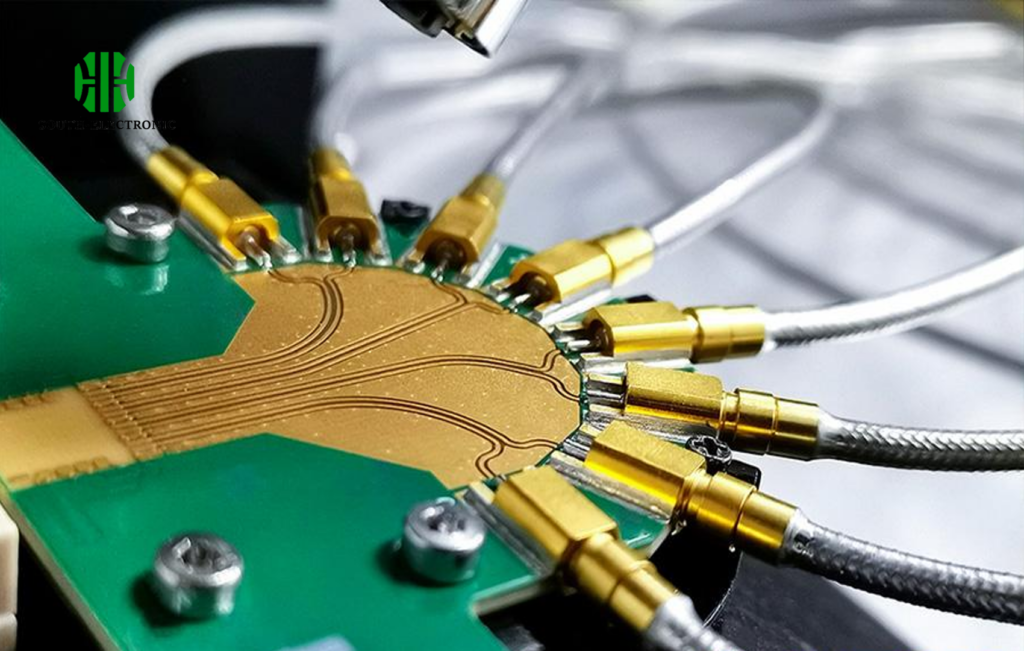
Are Carbon Ink Pads Reliable? 5 Cheap Alternatives to Standard Test Points!
Carbon ink pads tempt with low pricing but fail frequently. Failed tests and rework consume savings. Explore better alternatives!
Carbon ink pads often suffer poor adhesion and high resistance, causing unreliable contact. Five superior budget options exist: solder-tinned vias, exposed component leads, copper pour edges, brass eyelets, and laser-drilled micro vias.
Evaluating Reliability and Implementation
Carbon ink creates headaches through three main flaws:
- Resistance inconsistency (5-100Ω variations)
- Wear degradation after 20-50 test cycles
- Delamination from board flexing
Compare these to cost-effective substitutes:
| Alternative | Cost | Reliability | Best For |
|---|---|---|---|
| Solder-Tinned Vias | $0 (existing) | Excellent | Digital boards |
| Exposed Leads | $0 | Good | QFP/PLCC components |
| Copper Pour | $0 | Fair | Power circuits |
| Brass Eyelets | $0.002/point | Very High | Vibration-prone use |
| Micro Vias | $0.001/point | High | High-density designs |
Soldering exposed leads requires zero extra CAD work—just probe resistor legs! Vias dipped in solder provide robust metallurgy for cents. For under $20 per 1000 units, press-fit brass eyelets withstand 500+ test cycles. Micro vias created during drilling eliminate material costs. Avoid carbon inks except for non-critical voltage checks. Focus instead on these five alternatives to maintain testing integrity without inflating BOM costs.
How Many Test Points Are "Enough"?
Too few points create untestable "blind zones." Too many bloat costs. Find your sweet spot!
Aim for 100-120 test points per square foot of board space. Cover every net voltage, ground plane, clock signal, and component-free nodes. Complex designs need 5% more points per layer.
Calculating Minimum Requirements
Balance coverage with economy using these guidelines:
| Criteria | Minimum Points | Testing Goal |
|---|---|---|
| Power/Ground Nets | 4-6 per plane | Detect shorts/opens |
| Critical Signals | 1 per unique clock | Validate timing |
| Component Clusters | 2 per 10 components | Identify solder defects |
| Board Edge Zones | 3 per 2-inch span | Detect flex cracks |
First, tag all nets carrying power—missed connections here create catastrophic failures. Add probes for oscillators measuring signal integrity. For areas with dense ICs, allocate 1 point per 80 pins to catch bridged solder. High-reliability medical or automotive boards require 20% extra points around connectors. Reduce points for redundant ground planes. Prioritize accessibility near board edges—probing center requires costly fixtures. Total test point cost stays under $0.25/board when leveraging existing vias.
Conclusion
Implement economical PCB testing via low-cost solutions like modified vias and flying probes. Match points to complexity. Smart choices deliver reliable validation without excess spending.

