
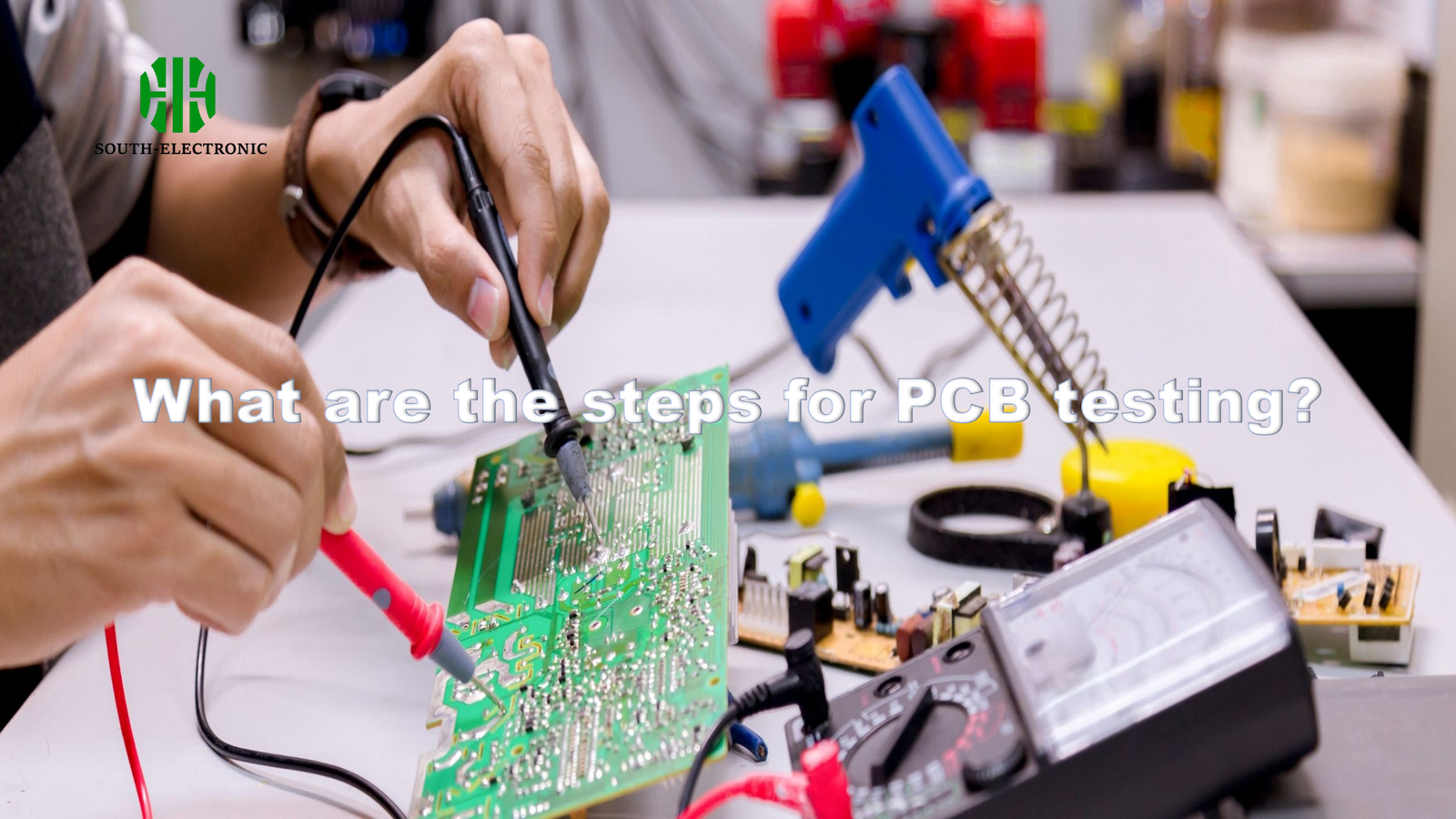
I spent weeks on a printed circuit board design only to see it fail after assembly. This frustrating setback taught me that proper PCB testing isn’t optional – it’s essential to avoid costly mistakes.
The core PCB testing[^1] steps are design review, bare board testing, component verification, functional testing, and environmental stress testing[^2]. This systematic approach catches flaws early and ensures your circuit board functions reliably under real-world conditions.

Getting the sequence right transformed my projects. What matters most is choosing the right methods for each stage. Let me share how I navigate these critical decisions.
How Do I Know Which PCB Testing Method to Use?
I once wasted $500 using automated optical inspection[^3] for simple prototypes. Choosing the wrong PCB test method burns time and money.
Match the testing approach to your board’s complexity and purpose. Critical medical devices need rigorous environmental testing while hobby projects may only require basic continuity checks.

Match Test Methods to Circuit Board Requirements
Not every project needs every test. You can break the decision into key factors:
| Board Type | Recommended Tests | Cost Impact |
|---|---|---|
| Basic prototypes | Visual inspection + continuity | Low |
| Medium complexity | Flying probe + functional | Medium |
| High-reliability | Boundary scan + thermal aging | High |
Start with your board’s purpose. My garden sensor project didn’t need burn-in testing, but my drone controller did. Component density changes everything too. Testing dense boards requires flying probe or automated X-ray inspection for hidden solder joints. Always consider failure consequences before selecting methods. A $10 toy PCB requires different testing than a $10,000 medical device. Production volume matters. I use in-circuit testing for big batches but boundary scan for small ones. Testing decisions affect time and costs, but skipping crucial steps leads to major failures. Focus on your board’s specific risks first.
How to Ensure PCB Durability?
My first automotive PCB cracked within 3 weeks. Environmental factors like vibration and humidity can destroy weak boards quickly.
Durability requires simulating real-world conditions. Environmental testing[^4] exposes hidden weaknesses through temperature cycling and vibration tests.
Three Pillars of Long-Lasting Circuit Boards
Long-term reliability combines design choices, manufacturing controls, and validation testing:
| Factor | Implementation | Key Tools |
|---|---|---|
| Material quality[^5] | Selecting TG170+ laminates | IPC-4101 compliance |
| Environmental tests | Thermal shock cycles (-40°C to +125°C) | Environmental chambers |
| Stress analysis | Vibration and bend testing | Finite element modeling |
Material selection makes the biggest impact. Standard FR4 fails during intense thermal cycling. I now use high-TG materials for automotive PCBs. Conformal coating helps too. This protective layer blocks moisture and reduces vibration damage. Test strategically instead of testing everything. Focused thermal cycling revealed my overheating component issue last month. Functional testing after environmental exposure shows true performance. Don’t forget the basics. Even humidity testing exposed dendritic growth on cheap boards I once made. Consistency creates durable products. Document every process step to identify weak points when boards fail.
How Much Does Professional PCB Testing Cost?
I nearly abandoned a project after receiving a $5,000 testing quote – but discovered lower-cost options through research.
Expect $50–$5,000+ depending on PCB complexity, quantity, and methods. A basic functional test costs much less than full environmental validation.
Breaking Down Circuit Board Testing Expenses
Testing costs[^6] depend on these interconnected factors:
| Cost Driver | Low-End Example | High-End Example |
|---|---|---|
| Test method | $50 (visual inspection) | $500 (boundary scan) |
| Board complexity | $100 (2-layer board) | $2,000 (16-layer HDI) |
| Volume discounts | $75/unit (10 pieces) | $15/unit (1,000+ pieces) |
Understand what you’re paying for. Expensive HALT testing replicates extreme conditions but isn’t needed for simple boards. Hidden costs hurt too. My first order had $500 setup fees I didn’t ask about. Bulk discounts matter. Ordering 10 prototypes doubles per-unit costs compared to 100-unit batches. DIY options reduce expenses for basic checks. I use a $30 multimeter for continuity tests instead of external labs. Always prioritize high-risk areas first. Testing power sections prevents catastrophic failures and saves refund expenses later.
Why Did My PCB Fail Testing and How to Fix It?
Seeing "FAIL" on my first production batch felt devastating – but revealed a cold solder joint[^7] issue that taught me invaluable lessons.
Common failures trace back to design flaws, manufacturing defects, or hidden component issues. Most circuit board problems are fixable with methodical checks.
Solving Circuit Board Testing Failures
Use failure type to identify solutions fast:
| Failure Type | Diagnosis Method | Solution |
|---|---|---|
| Short circuits | Thermal imaging or test points | Inspect solder bridges, component placement |
| Open circuits | Continuity testing | Check traces for breaks, reflow solder |
| Component malfunction | Functional test isolation | Replace components, verify datasheets |
| Environmental weakness | Post-stress inspection | Improve conformal coating, material grade |
Always start with basics. Power issues caused 60% of my early failures. Measure voltages before diagnosing complex faults. Document everything. Logging failure locations revealed my manufacturing partner’s soldering machine fault last month. Component-level isolation works best. Swap suspected ICs to confirm failures. Many problems originate in design. My impedance mismatch issue required trace width adjustments rather than component changes. Environmental stress identifies weaknesses missed during functional checks. Test boards under actual operating conditions when possible.
Conclusion
Proper PCB testing requires multiple stages: verification checks before production and validation tests under real conditions. This process prevents expensive failures and creates reliable electronics efficiently.
[^1]: Understanding PCB testing best practices can help you avoid costly mistakes and ensure reliable circuit board performance.
[^2]: Exploring environmental stress testing will provide insights into how to ensure your PCB can withstand real-world conditions.
[^3]: Learning about automated optical inspection can help you determine if it’s the right choice for your PCB testing needs.
[^4]: Explore this link to understand how environmental testing can reveal weaknesses in PCBs and enhance their durability.
[^5]: Learn about the impact of material quality on PCB durability and how to choose the right materials for long-lasting performance.
[^6]: Discover the various factors influencing PCB testing costs and find budget-friendly options for your projects.
[^7]: Understanding cold solder joints is crucial for PCB reliability. Explore this link to learn effective repair techniques and prevention strategies.

