
What is PCB Reflow?
Reflow soldering forms critical PCB connections. Learn how temperature control prevents defects like cold joints, component drift & board warping. Optimize profiles with thermal sensors!
What is a Tooling Hole in a PCB?
PCB tooling holes are vital for mounting hardware, PCB stability, manufacturing alignment, and test fixtures. Design standards prevent failures; detail is critical for mfg success.
How to master PCB stackup design?
Master PCB stackup design: factors like cost, signal layers, EMI reduction & symmetry. Key principles for impedance control, power-ground coupling & layer arrangement in multilayer boards.
What are the standards for PCB pad design?
PCB pad design standards prevent defects: min pad size 0.25mm, max 3x aperture, shapes like oval/rectangular. Avoids soldering failures, production delays, scrap costs. Optimizes reliability and efficiency.
What are the reasons for poor etching of PCB boards?
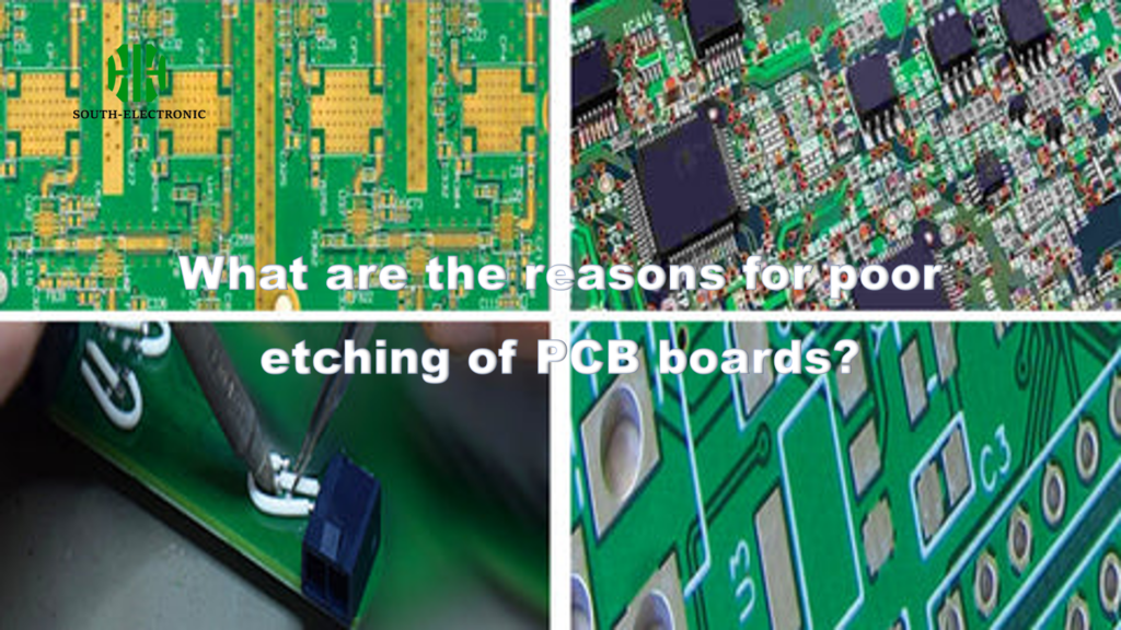
Ensure etching quality in PCB manufacturing to prevent incomplete etching, side etching, etching interlayer, over-etching, and dry film bite. Optimize parameters, maintain equipment, and train staff for high yield and reliability.
