Master PCB via selection: balance cost, density & signal needs. Proper sizing prevents overheating. Understand via-pad differences. Prevent failures with plating standards.

Master PCB via selection: balance cost, density & signal needs. Proper sizing prevents overheating. Understand via-pad differences. Prevent failures with plating standards.
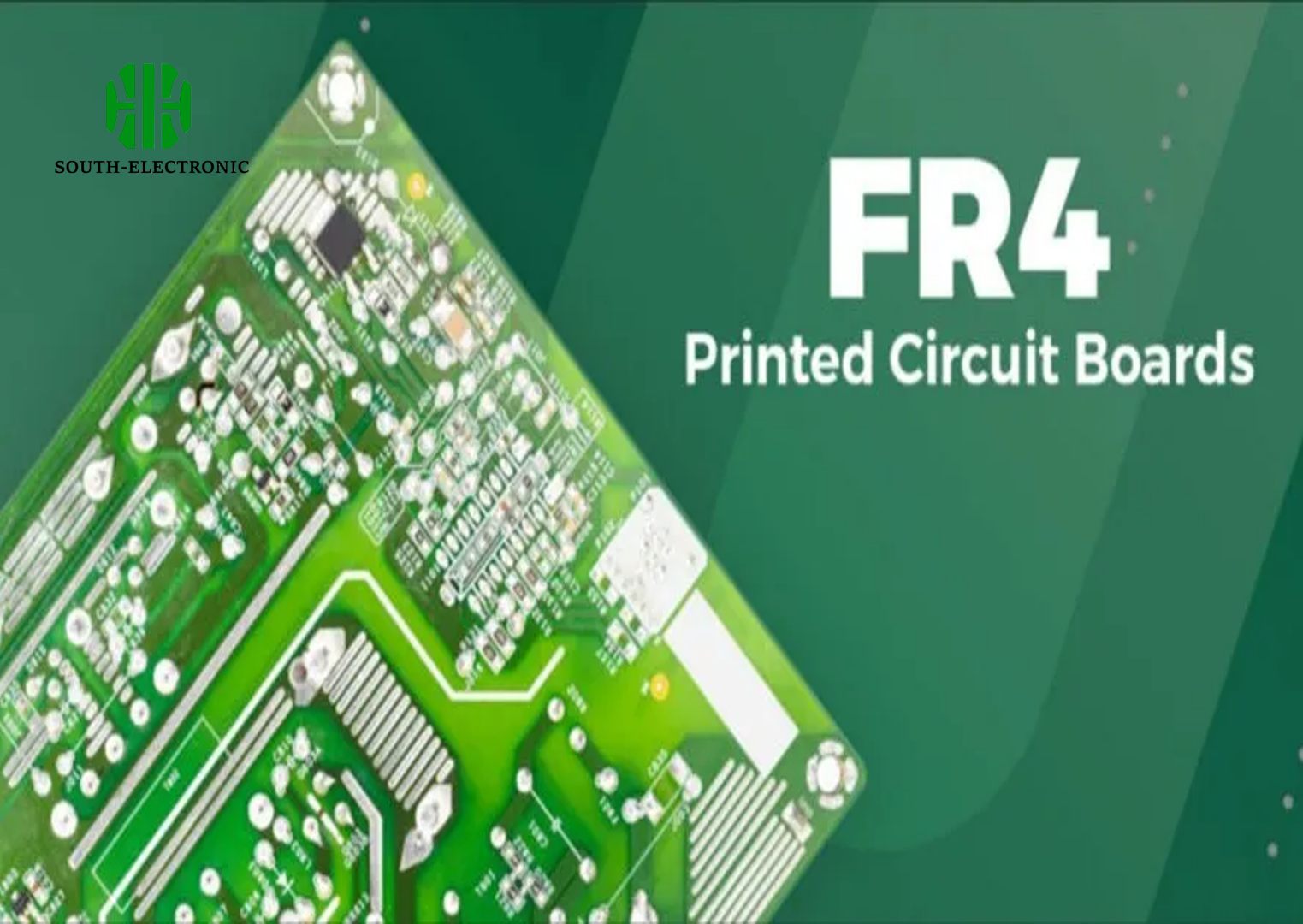
FR-4 supports MHz designs affordably but suffers dielectric losses >5GHz/long traces. Optimize layer stackup, thermal design & shielding – or switch to low-loss laminates for

Choose IC packages by balancing signal speed, heat dissipation, board space, and cost. Avoid overheating and failures—learn key uses for BGA, QFN, QFP & SOT
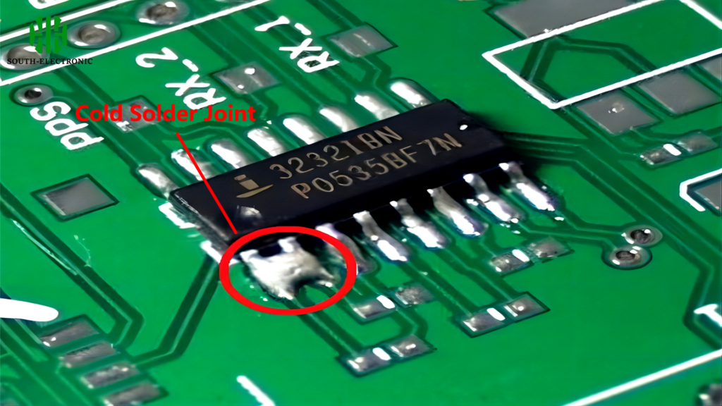
Cold solder joints cause device failure. Learn to spot dull/cracked joints, fix with proper reflow and tools like flux, and test using thermal/multimeter methods.
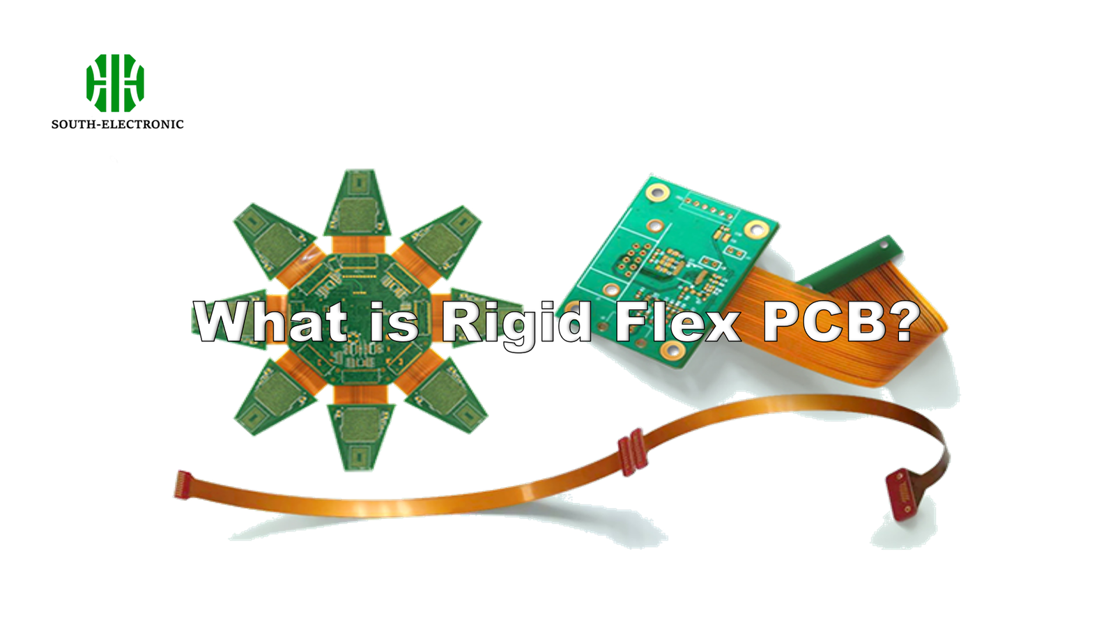
Rigid flex PCBs merge solid & bendable circuits to eliminate connectors, cut failure risks, boost signal integrity, and enable compact designs for medical/aerospace systems.
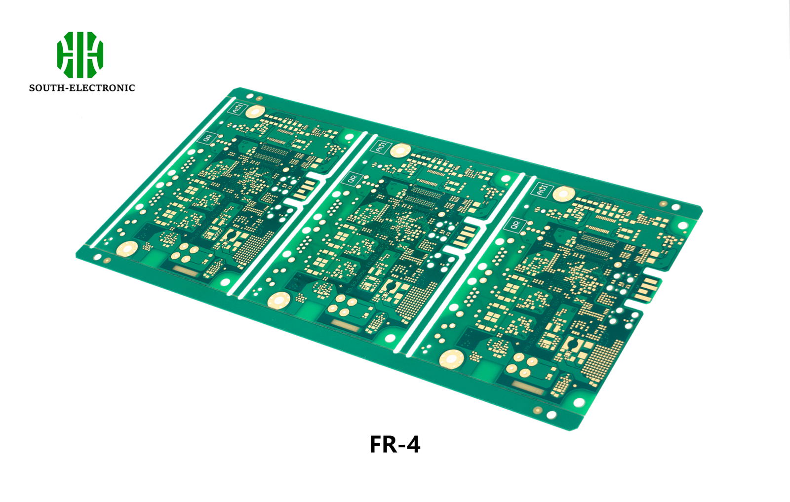
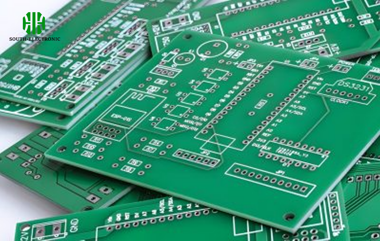
FR4 PCB material dominates with 5 key traits: insulation, strength, flame retardancy (UL-certified), moisture resistance, and cost-efficiency. Avoid catastrophic failures by mastering specs.

Optimize standard PCB panel sizes (18×24″, 12×18″) to cut costs. Choose breakaway methods wisely, minimize material waste, and avoid design errors to maximize yield and
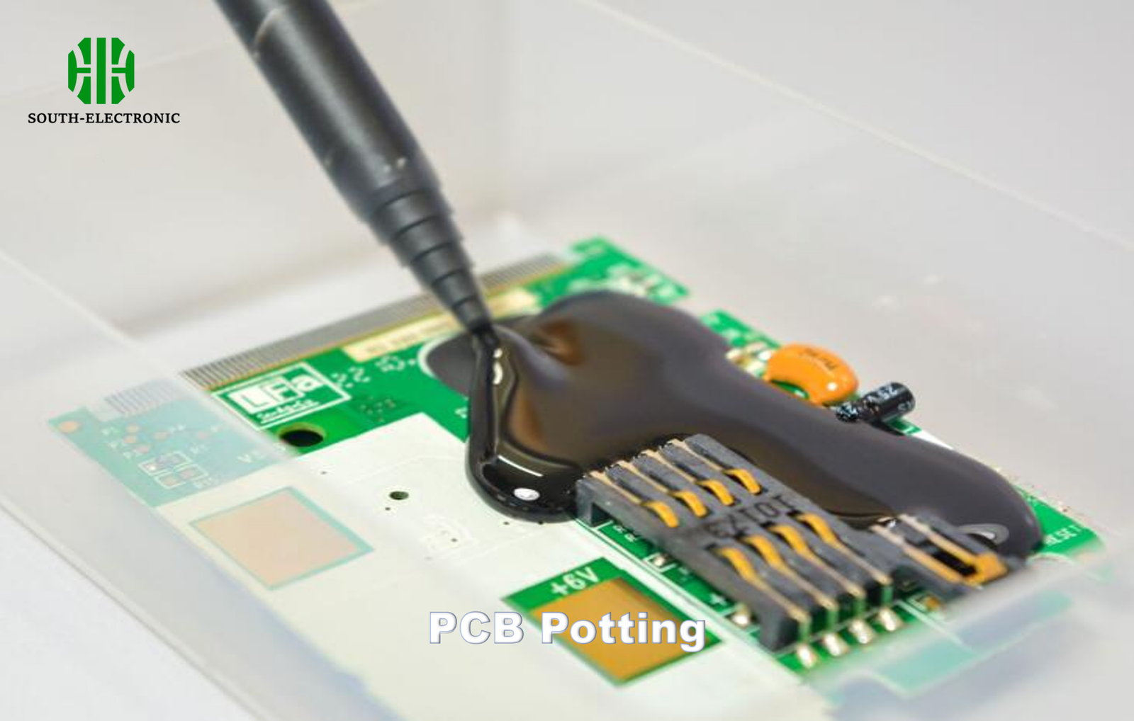
PCB potting seals assemblies in resin for extreme environment protection. Learn potting vs. conformal coating selection, process tips to prevent voids/cracks, and avoid hidden costs.
3-layer PCBs cost more than 2-layer & often less reliable than 4-layer. Understand hidden manufacturing expenses,thermal risks, & rare use cases before choosing layers.
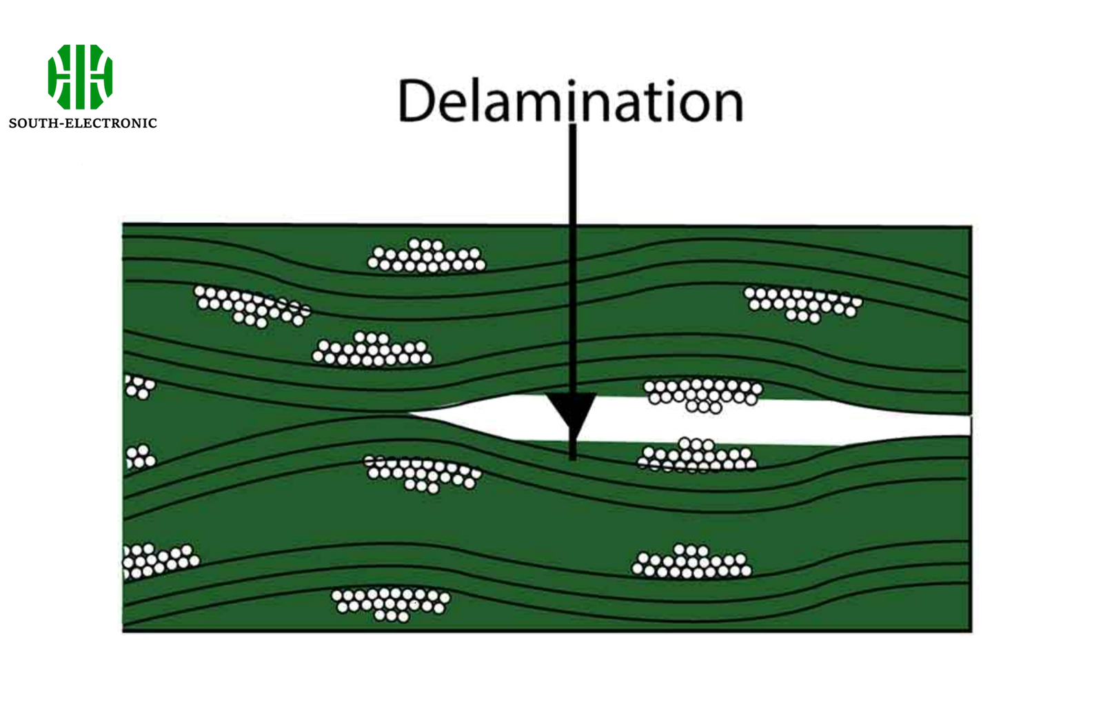
Choose PCB laminates wisely: Upgrade FR-4 for GHz signals or extreme heat. Prevent delamination/CAF via precise lamination. Balance 6 thickness factors for reliability. Stop failures