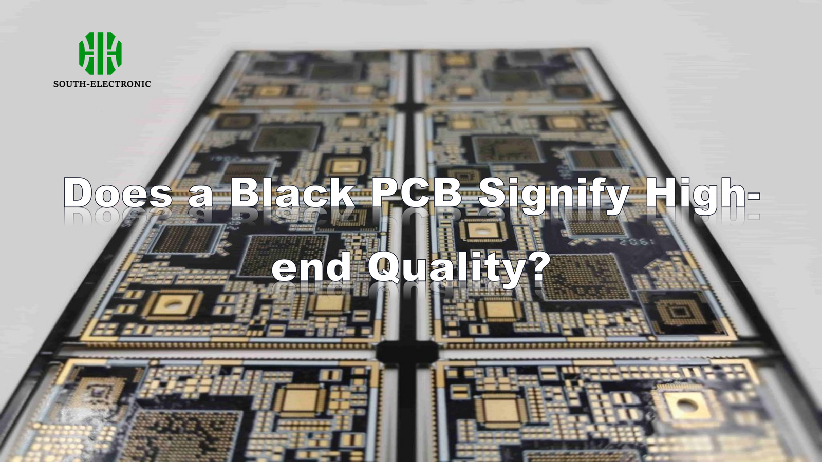
Black PCBs aren’t inherently premium. Quality depends on manufacturing, material grades, and design specs—not color. Avoid for high-inspection or budget projects; use only for aesthetics.

Black PCBs aren’t inherently premium. Quality depends on manufacturing, material grades, and design specs—not color. Avoid for high-inspection or budget projects; use only for aesthetics.
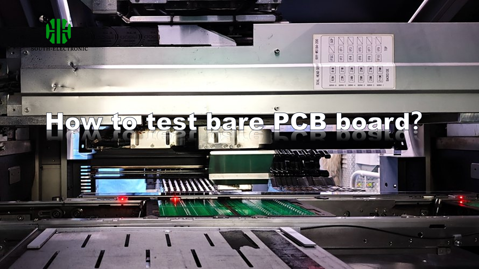
Test bare PCBs with flying probe, AOI, and impedance meters to catch hidden flaws early. Balance materials, tolerances, and layer count to control costs and
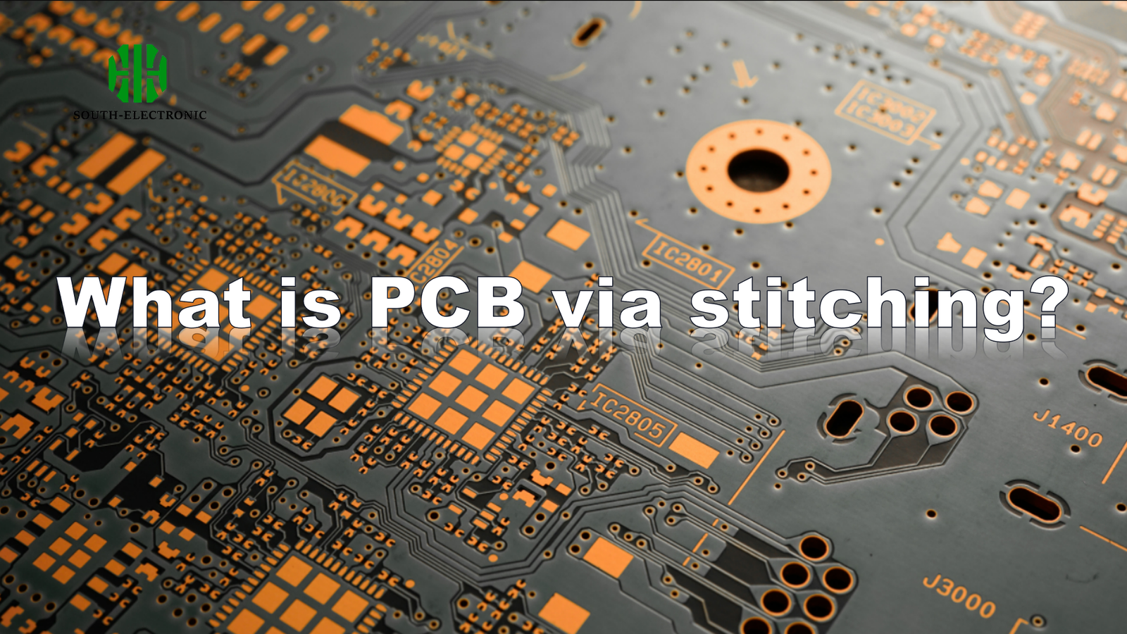
PCB via stitching creates parallel return paths to suppress EMI and boost signal integrity in high-speed designs, but overuse risks PCB fractures during manufacturing—balance is
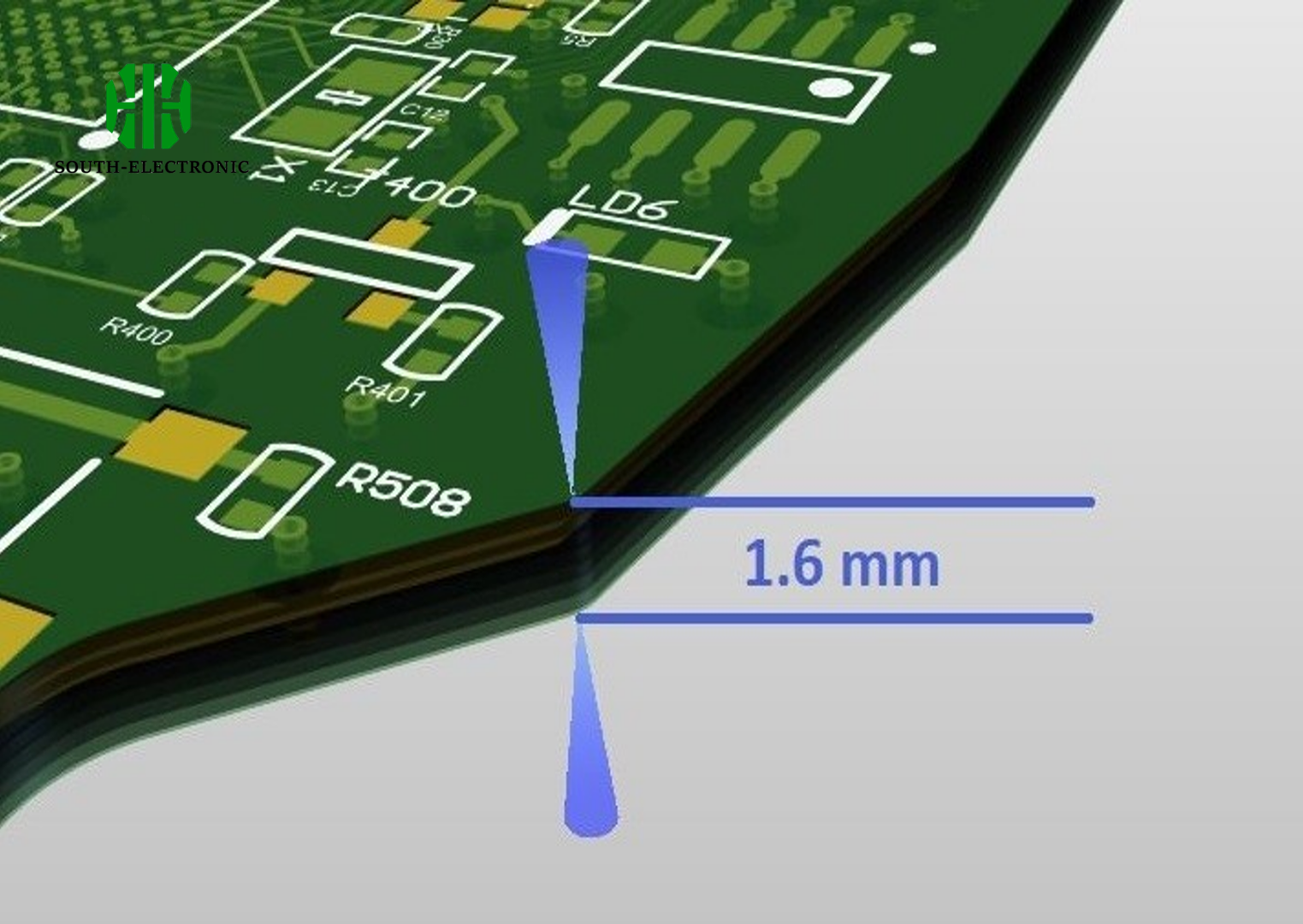
1.6mm PCB thickness balances rigidity, cost & SMT reliability. Thinner boards risk warping; thicker add bulk. Choose based on mechanical stress, layers & thermal needs.
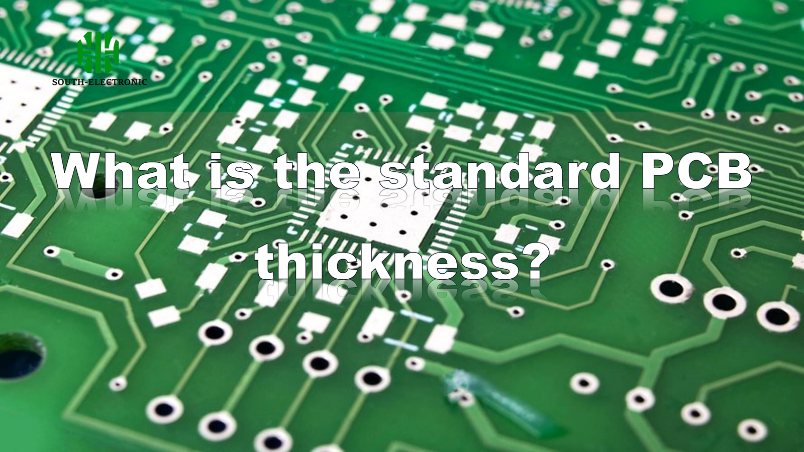
PCB thickness impacts reliability & cost. Default is 1.57mm for compatibility. Choose 1mm for wearables or 2.36mm+ for high-power/industrial. Mind layers, signals & heat.
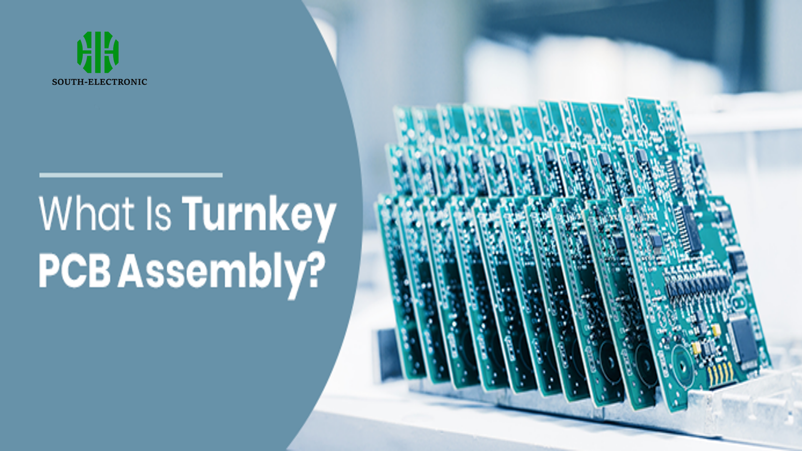
Eliminate supplier chaos! Turnkey PCB assembly manages everything from parts sourcing to shipment for your electronic products. Faster time-to-market, reduced risk, and simplified scaling. Perfect
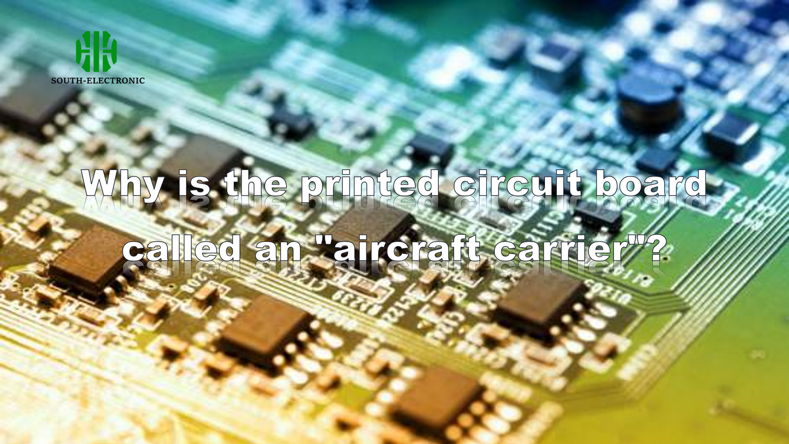
Printed circuit boards (PCBs), invented by Paul Eisler, are essential “electronic aircraft carriers.” They reduce wiring errors, enable automation & miniaturization, and underpin all modern

Master star grounding to silence PCB noise! Learn routing tricks for single/multi-layer boards, avoid 6 critical grounding mistakes, and crush EMI with proven techniques.

Solve PCB disconnect headaches! Choose spring contacts (pogo pins, fingers, cantilevers) matched to mechanical demands. Optimize layout & prevent failures for stable connections.
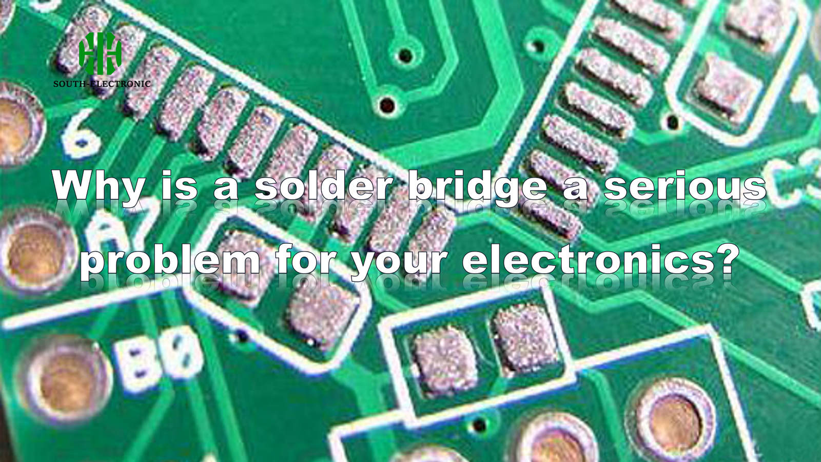
Prevent catastrophic PCB failures: Learn critical solder bridge avoidance strategies in design spacing, solder mask barriers, reflow controls, and AOI inspection to save costs.