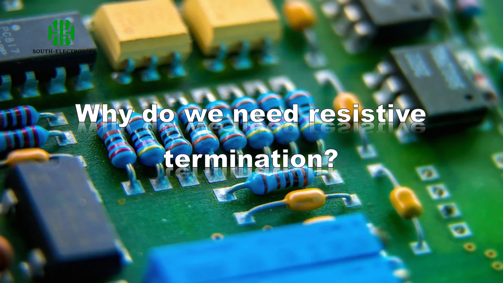
Master resistive termination techniques—parallel, series, Thevenin—to eliminate reflections, noise, and data errors. Essential solutions for reliable signal integrity and robust PCB design.

Master resistive termination techniques—parallel, series, Thevenin—to eliminate reflections, noise, and data errors. Essential solutions for reliable signal integrity and robust PCB design.
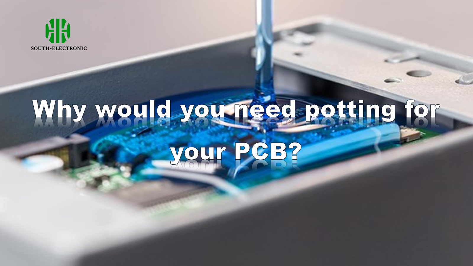
Potting protects PCBs from moisture, vibration, and shocks. Choose epoxy, silicone, or polyurethane compounds based on your environment. Balance cost and durability for long-lasting boards.
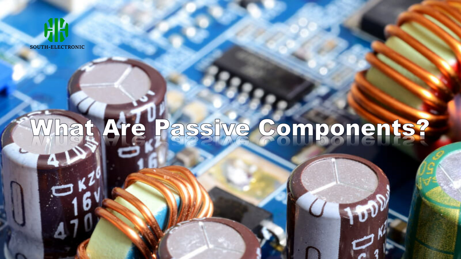
Passive components are essential, power-free circuit heroes. Resistors control current, capacitors store charge, inductors manage fields. Learn types, differences vs active, and key selection strategies.
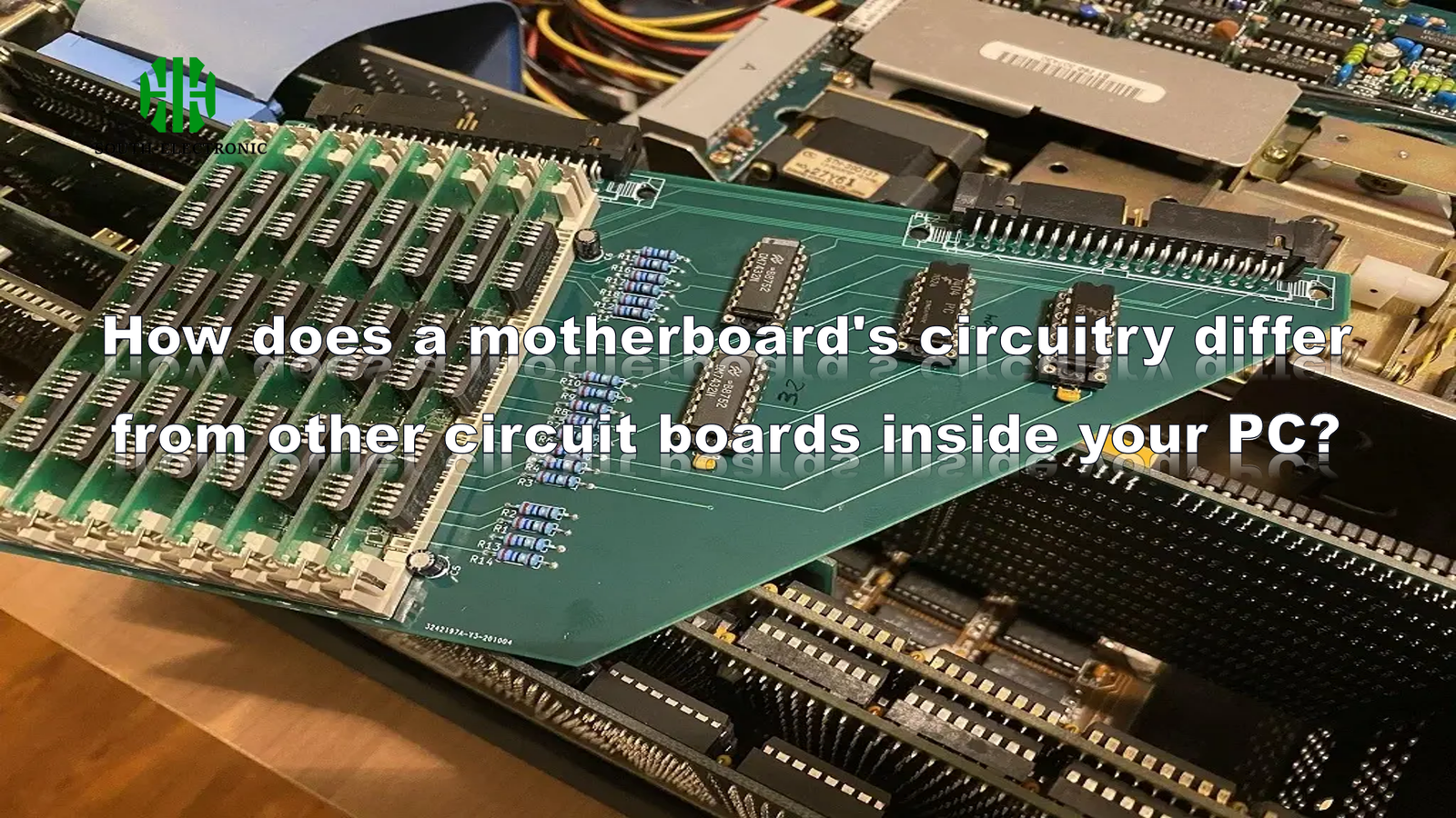
Motherboards are vital PC hubs. Their complex circuits manage power delivery to CPU/RAM, high-speed data transfer, & precise timing. Chipsets coordinate everything, requiring layered PCBs.
Understand why PCB prototype milling costs more than mass production. Learn key drivers: volume, automation, materials. Optimize costs for every scale with smart equipment and
Analyzes leakage plating & false leakage plating in PCB immersion gold process. Causes include poor pretreatment, plating solution imbalance, conductivity issues, incorrect parameters, and mask
Microcontrollers (MCU) integrate CPU, memory & peripherals for dedicated tasks like car airbags or thermostats. Use $10 budget chips (ESP32/Arduino) for pro projects. Source suppliers

Essential guide to PCB letters: R=Resistor, C=Capacitor, Q=Transistor, D=Diode. Numbers indicate circuit function & component position. Decode R107, C118 effortlessly!

Master PCB substrates: Avoid failures by choosing correct materials (FR-4, metal core, HF) for apps like automotive, medical & sourcing from trusted suppliers. Build durable

FPGAs deliver insane parallel speed for AI, robotics, and networks. Start with $20 boards. Beat CPUs/GPUs in power and latency. Essential career skill for 5G,