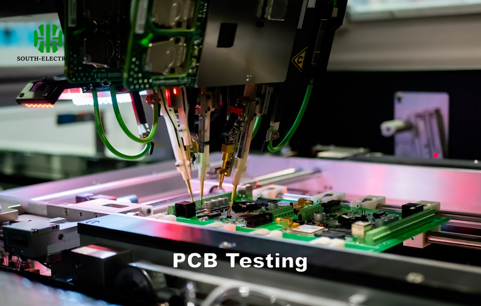
Choose the right PCB test method to prevent costly failures. Learn which test (ICT, Flying Probe, AOI) fits your volume, budget, and complexity. Avoid defects,

Choose the right PCB test method to prevent costly failures. Learn which test (ICT, Flying Probe, AOI) fits your volume, budget, and complexity. Avoid defects,
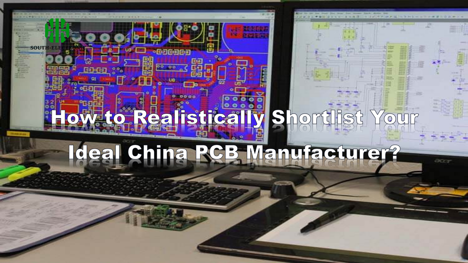
Avoid China PCB partner pitfalls: demand full cost transparency, validate Gerber files rigorously & cultivate multi-site resilience. Prioritize technical skill over lowest price.
Choose LGA over BGA for cheaper repairs, easier visual inspection & thermal efficiency. Ideal for desktops/servers needing upgrades without performance loss. Cut manufacturing costs &

Choose LGA over BGA for cheaper repairs, easier visual inspection & thermal efficiency. Ideal for desktops/servers needing upgrades without performance loss. Cut manufacturing costs &
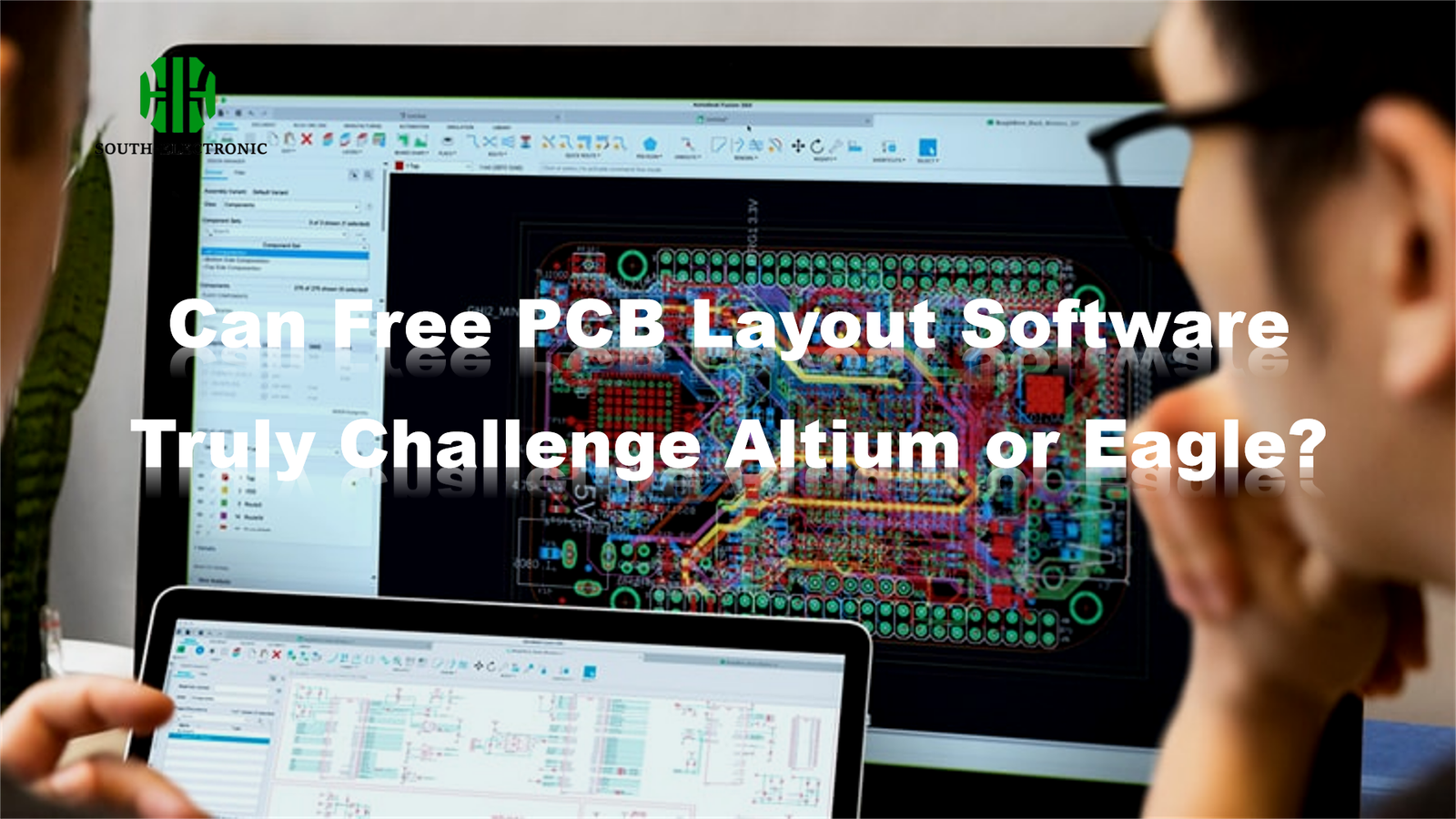
Free PCB design software helps beginners start affordably but struggles with complex projects. Learn key limitations & smart workarounds to leverage free tools effectively for
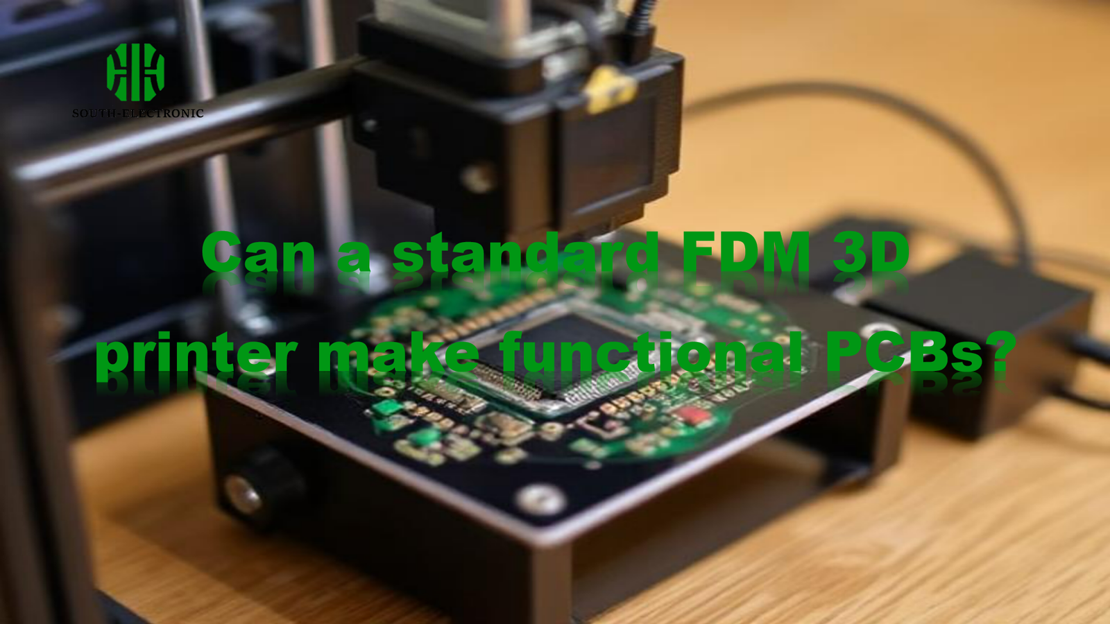
FDM printing creates quick DIY PCBs with conductive filament, ideal for low-power prototypes despite trace/soldering limits. Explore methods for faster, cheaper iterations.
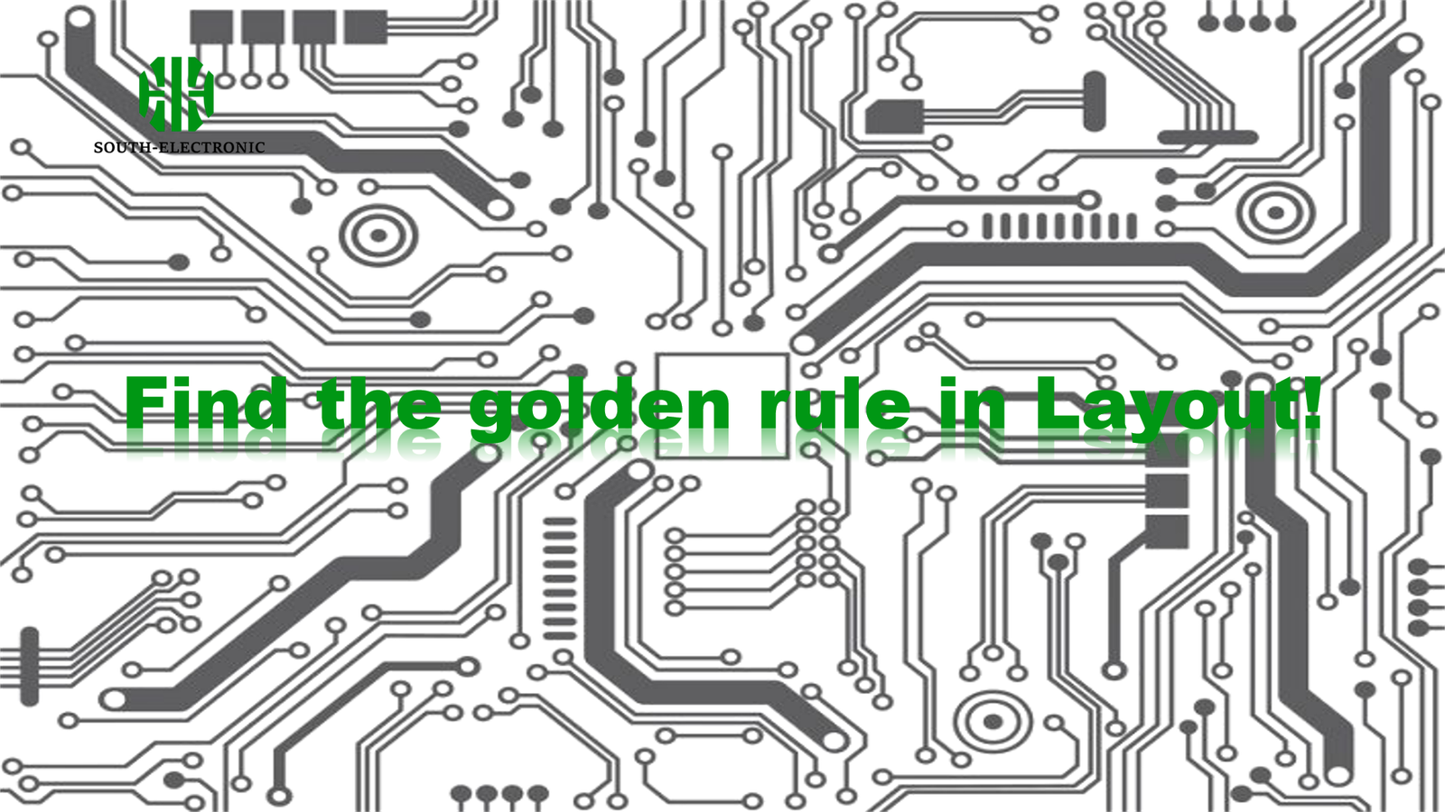
Top 10 PCB design rules for optimal layout and manufacturing: grid selection, routing, power planes, component grouping, panelization, DRC, silkscreen, capacitors. Boost reliability and cut

Automated optical inspection (AOI) cuts PCB errors by 95% vs manual checks. Learn AOI vs SPI vs AXI cost/ROI comparisons, false alarm fixes, and key
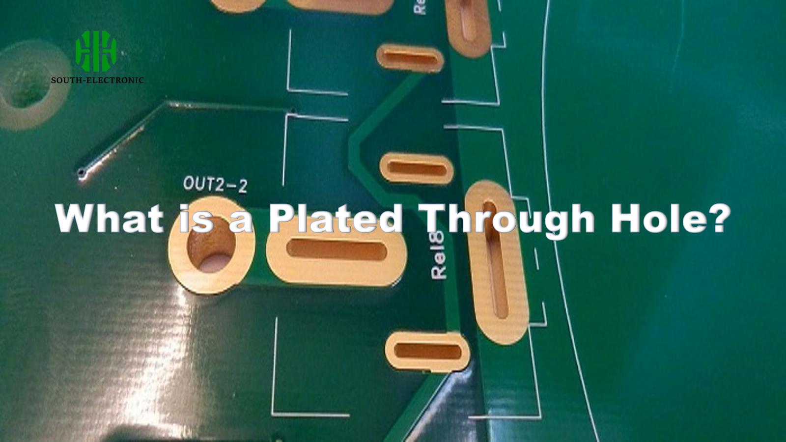
Plated Through Hole (PTH) technology uses copper-lined holes to create reliable electrical connections between PCB layers, preventing signal failures & strengthening component mounts. Vital for
Safely clean PCBs without damage using manual brushing with isopropyl alcohol, distilled water rinsing, and thorough drying. Avoid ultrasonic risks targeting corrosion and residues.