Skip to content
HOME
ABOUT
Company Profile
Factory Equipment
Quality Control
Certificates
Process Capability
Corporate Culture / Mission & Vision
PCB
FR4 PCB
Single Layer PCB
Double Layer PCB
4 Layer PCB
6 Layer PCB
8 Layer PCB
Multilayer PCB
Rigid PCB
PCB Fabrication
PCB Prototyping
High TG PCB
HDI PCB
Flex PCB
Flex PCB Fabrication
Rigid-Flex PCB
High Frequency PCB
Rogers PCB
PTFE PCB
Advanced PCB
Thick Copper PCB
Backplane PCB
Metal Core PCB
Ceramic PCB
Alumina PCB
Aluminum Nitride PCB
PCBA
Turnkey PCB Assembly
PCB Assembly (SMT & THT)
Box Build & Final Assembly
INDUSTRIES
IoT & Smart Devices PCBA
IoT Devices PCBA
IoT Gateway PCBA
Edge IoT PCBA
Wireless IoT PCBA
Industrial & Automation PCBA
Industrial Control PCBA
PLC Control PCBA
Motor Drive PCBA
Industrial Power Supply PCBA
Automotive Electronics PCBA
Automotive ECU PCBA
ADAS PCBA
EV Charger PCBA
BMS PCBA
LED & Power Electronics PCBA
LED Lighting PCBA
High Power LED PCBA
UV LED PCBA
LED Driver & Power Supply PCBA
Robotics & Motion Control PCBA
Robot Control PCBA
Motion Control PCBA
Servo Drive PCBA
Telecom & Networking PCBA
Telecom Equipment PCBA
Network Equipment PCBA
RF Module PCBA
High-Speed Digital PCBA
Aerospace & Defense PCBA
Aerospace Electronics PCBA
Defense Electronics PCBA
High-Reliability PCBA
Medical Electronics PCBA
Medical Device PCBA
Patient Monitoring PCBA
Medical Power Supply PCBA
RESOURCES
Technical Resources
Knowledge Base
Downloads
Case Studies
Blog
FAQ
CONTACT
Quote Now
PCB Blog & Engineering Resources
Practical PCB design, manufacturing, and assembly insights to help engineers build reliable products.
Search
Search
Popular Articles
PCB Design
,
PCB Manufacturing
July 7, 2024
How to Improve the PCB Layout Level?
March 26, 2025
What is PCB Art?
August 17, 2024
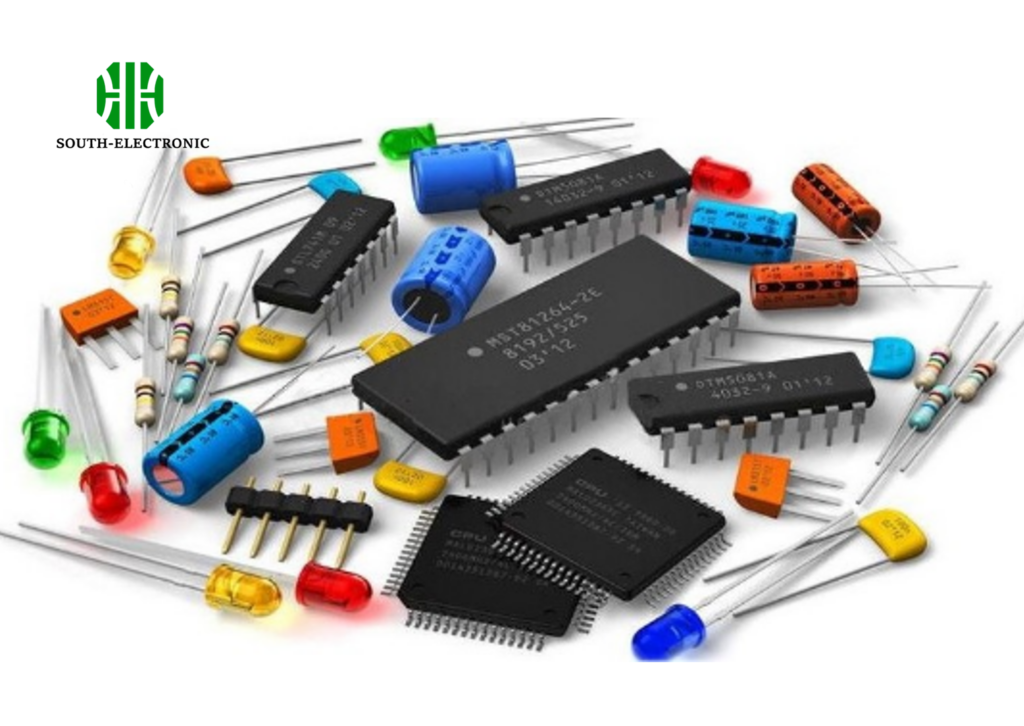
Electronic Component Basics: List of Components And It Functions
May 28, 2024
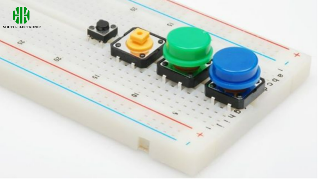
PCB Buttons: What They Do and How to Use Them
PCB Design
What is via filling?
Why is a solder bridge a serious problem for your electronics?
My PCB is Warped! Can I Fix It?
What Are the Most Common Causes of PCB Failure?
What is a Short Circuit?
PCB Tombstone: What Is It and How to Avoid It?
View more about PCB Design →
PCB Materials
How to Select the Right CCL for Your Application?
Where should capacitors be placed on your PCB?
What Are the Key Advantages and Disadvantages of BGA Packages?
What Are Chip-on-Board LEDs? A Comprehensive Look at Compact LED Technology
View more about PCB Materials →
PCB Assembly
What is the purpose of PCB via filling?
How do you master the basics of soldering wire on a circuit board?
Can you solder wires to PCB?
What are the different types of solder mask materials?
What are important considerations for BGA fanout design?
How do you solder wire to a circuit board?
View more about PCB Assembly →
PCB Manufacturing
What should you know about solder mask material?
Your PCB Material Dilemma: Do We Have the Answers?
What is the Function of Solder Mask?
Does PCB require soldering?
What is BGA Fanout?
What is Copper Clad Laminate?
View more about PCB Manufacturing →
PCB Quality & Testing
What Exactly Can PCB X-Ray Inspection Detect?
Is the Quality Compromised with Quick Turn PCBs?
What are the common types of Test PCBs?
What are common types of low-cost PCB test points?
How many PCB testing methods do you know?
What Are Low-Cost PCB Test Points?
View more about PCB Quality & Testing →
Industry Insights
Top 10 PCB Manufacturers in Northern Europe in 2026
Top 10 PCB Manufacturer of Mexico in 2026
Top 10 PCB manufacturers in Saudi Arabia in 2026
Top 10 PCB manufacturers In Russia In 2026
Top 10 PCB manufacturers in Korea in 2026
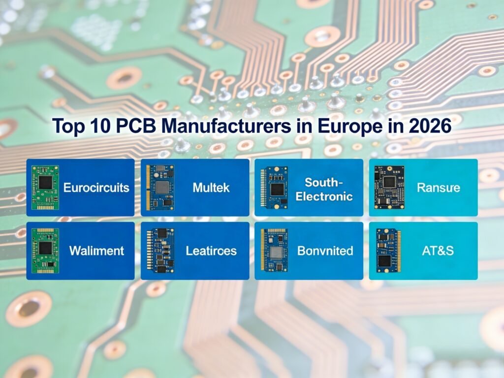
Top 10 PCB Manufacturers in Europe in 2026
View more about Industry Insights →
Company News
South-Electronic September Promotion
South-Electronic—Leading electronic manufacturing service provider
Spring Festival Holiday Notice
The Golden Snake starts fortune and develops vigorously
This Christmas is lit up by technology!
Mid-Autumn Festival Holiday Notice
View more about Company News →
Latest Posts
April 9, 2026
Top 10 PCB Manufacturers in Northern Europe in 2026
April 7, 2026
Top 10 PCB Manufacturer of Mexico in 2026
April 2, 2026
Top 10 PCB manufacturers in Saudi Arabia in 2026
March 31, 2026
Top 10 PCB manufacturers In Russia In 2026
March 26, 2026
Top 10 PCB manufacturers in Korea in 2026
March 24, 2026
Top 10 PCB Manufacturers in Europe in 2026
Upload Gerber & Get Quote
WhatsApp us
Send Us a Message
The more detailed you fill out, the faster we can move to the next step.
Subject
PCB Only
PCBA / Turnkey Assembly
Components Sourcing Only
Others
Name
Email
Message
Gerber, BOM, or reference files are welcome.
Get A Quote