Master 8-layer PCB stackups: Optimize configurations for high-speed/mixed signals. Precisely calculate impedance and thickness. Cut costs by 30% with material and design hacks.

Master 8-layer PCB stackups: Optimize configurations for high-speed/mixed signals. Precisely calculate impedance and thickness. Cut costs by 30% with material and design hacks.
Free step-by-step PCB design guide for beginners: Learn software selection, avoid fatal layout errors, and prepare manufacturing files correctly to save time & money.

Master 7 PCB assembly stages to avoid delays. Choose IATF/ISO-certified manufacturers for medical/auto projects, fix critical design errors early & know when to switch from

Diagnose & prevent common PCB failures: manufacturing flaws, environmental stress, soldering defects. Learn visual inspection, repair techniques & cost-effective solutions.
Avoid SMT prototype fails! Top defects (tombstoning, bridging, BGA issues) with fixes. Key: design audits, communication with assembly shops & pre-testing. Save costs & time.

Discover why PCB traces fail—impedance issues, overheating—and how to fix them. Learn trace design factors, troubleshooting steps, and tools for reliable circuits.
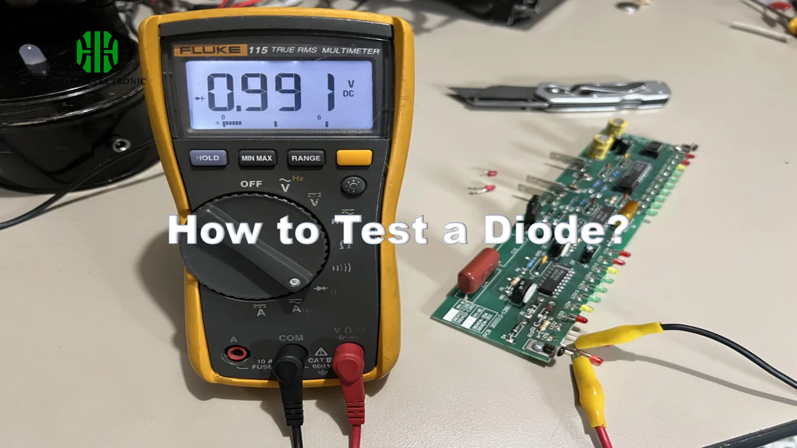
Learn to test diodes with any multimeter: Set to diode/resistance mode, probe anode/cathode. Identify healthy (0.5-0.8V drop) vs faulty diodes (shorted/open/leaky). Prevent circuit failures with
Radar PCBs enable critical detection from storm tracking to touchless devices. Discover innovations in materials, ruggedization & cost reduction driving weather & consumer applications.
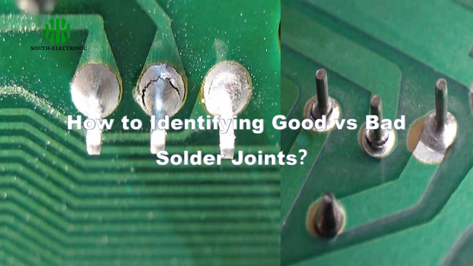
Spot shiny, smooth solder joints; avoid dull, cracked ones. Use correct solder/flux for electronics or plumbing to prevent failures and save costs. Master inspection for

Master PCB via design: Choose blind/buried vias for dense layouts, calculate size/spacing to prevent overheating, and avoid common failure causes. Essential for modern circuit reliability.