PCB pad design standards prevent defects: min pad size 0.25mm, max 3x aperture, shapes like oval/rectangular. Avoids soldering failures, production delays, scrap costs. Optimizes reliability

PCB pad design standards prevent defects: min pad size 0.25mm, max 3x aperture, shapes like oval/rectangular. Avoids soldering failures, production delays, scrap costs. Optimizes reliability

Ensure etching quality in PCB manufacturing to prevent incomplete etching, side etching, etching interlayer, over-etching, and dry film bite. Optimize parameters, maintain equipment, and train

Cross-split in PCB design disrupts signal return paths, causing impedance issues, EMI, and crosstalk. Mitigate via stitching capacitors, cross-line bridging, and high-speed routing best practices.
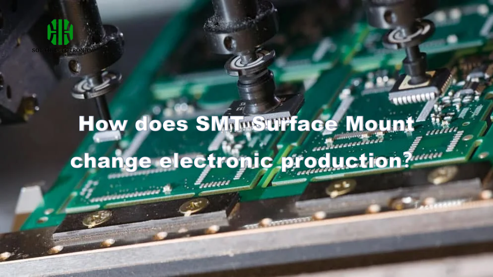
cheaper production, full automation & tiny devices enabled. See how surface mount revolutionized manufacturing forever.

Identify PCB connector type & lock first! Use precise tools – solder tools for soldered joints, gentle leverage for mounted. Avoid force; patience prevents board
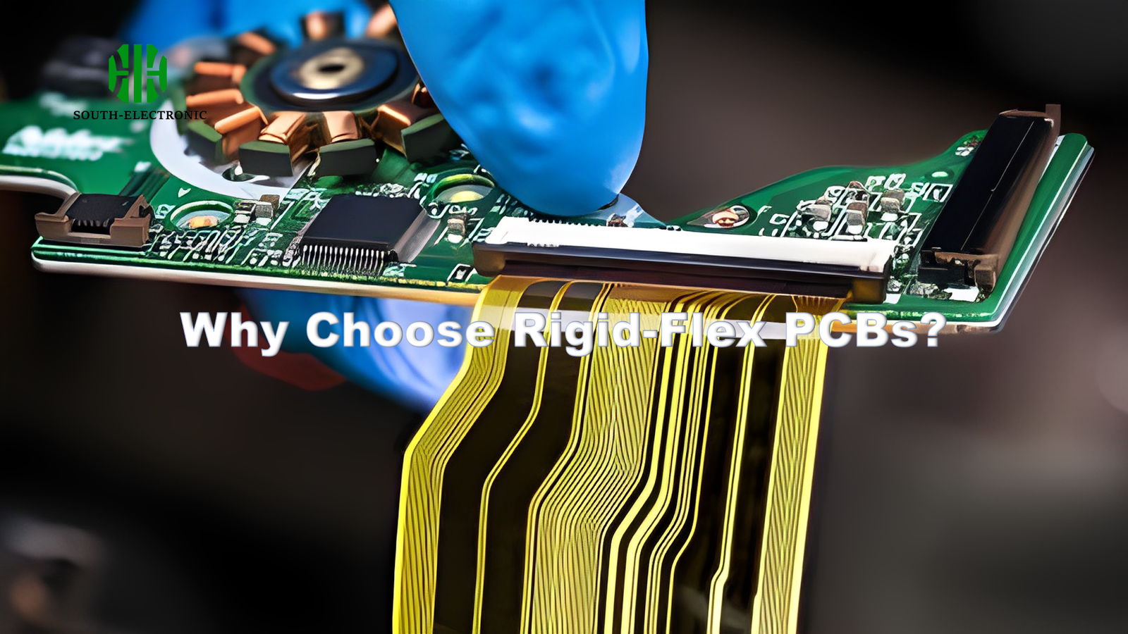
Las PCB rígido-flexibles combinan circuitos rígidos y flexibles, ahorrando un 60 % de espacio y mejorando la resistencia a vibraciones e impactos para dispositivos portátiles,

No universal “best” SMT pick and place machine exists. Your ideal choice depends on production volume, component complexity, precision needs, and budget for efficient assembly.

Discover QFN packages: ideal for compact devices with superior heat dissipation. Compare QFN, QFP, TQFP, DFN and variants (VQFN, LQFN, WQFN) to prevent soldering failures

Explore how multi-layer PCB stackups, premium laminate materials, and precision VRM designs ensure graphics card stability during extreme overclocking and 4K rendering.
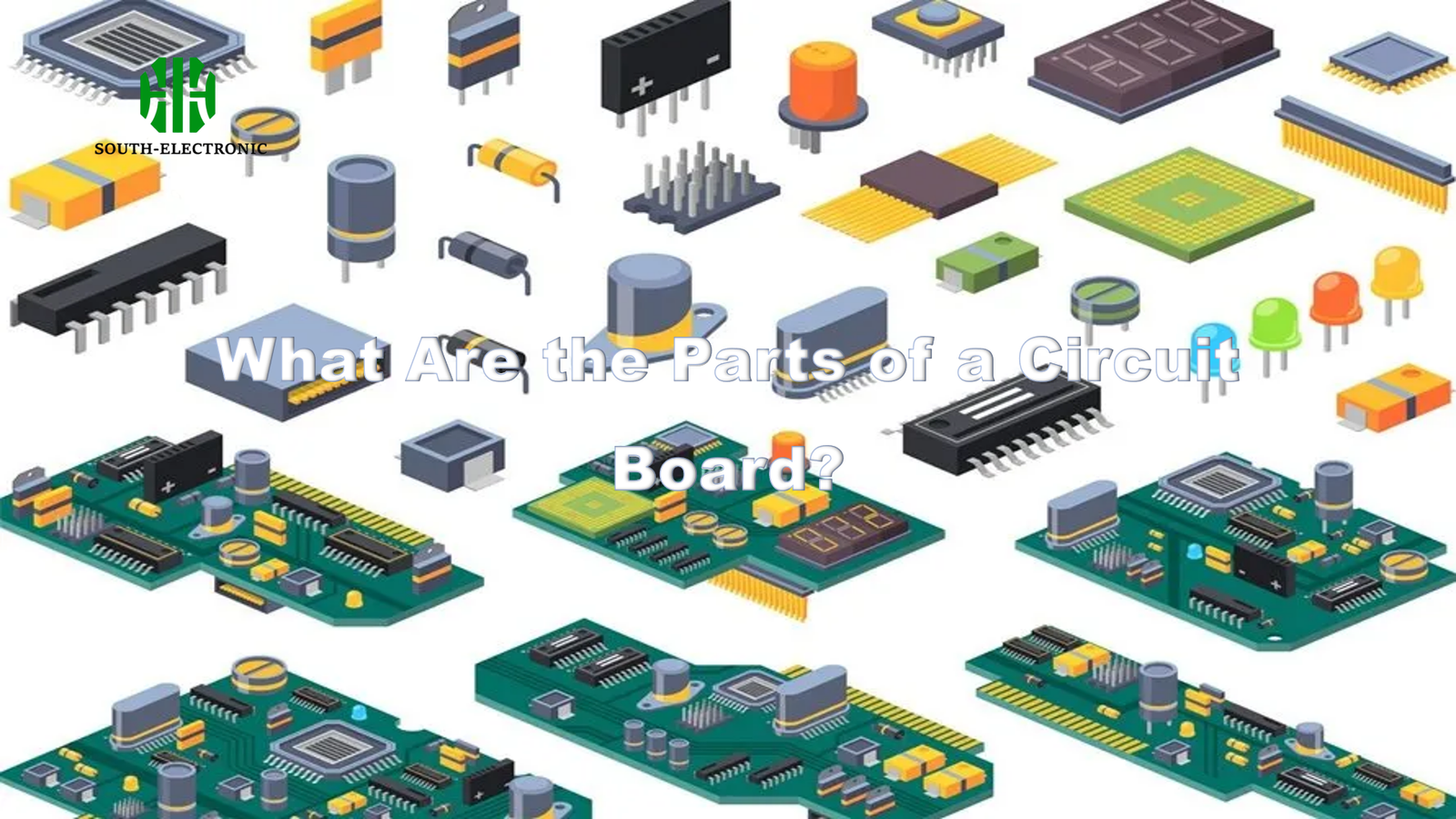
Learn to identify key circuit board parts like resistors, capacitors, and ICs. Understand symbols and functions to troubleshoot electronics confidently. No more confusion!