
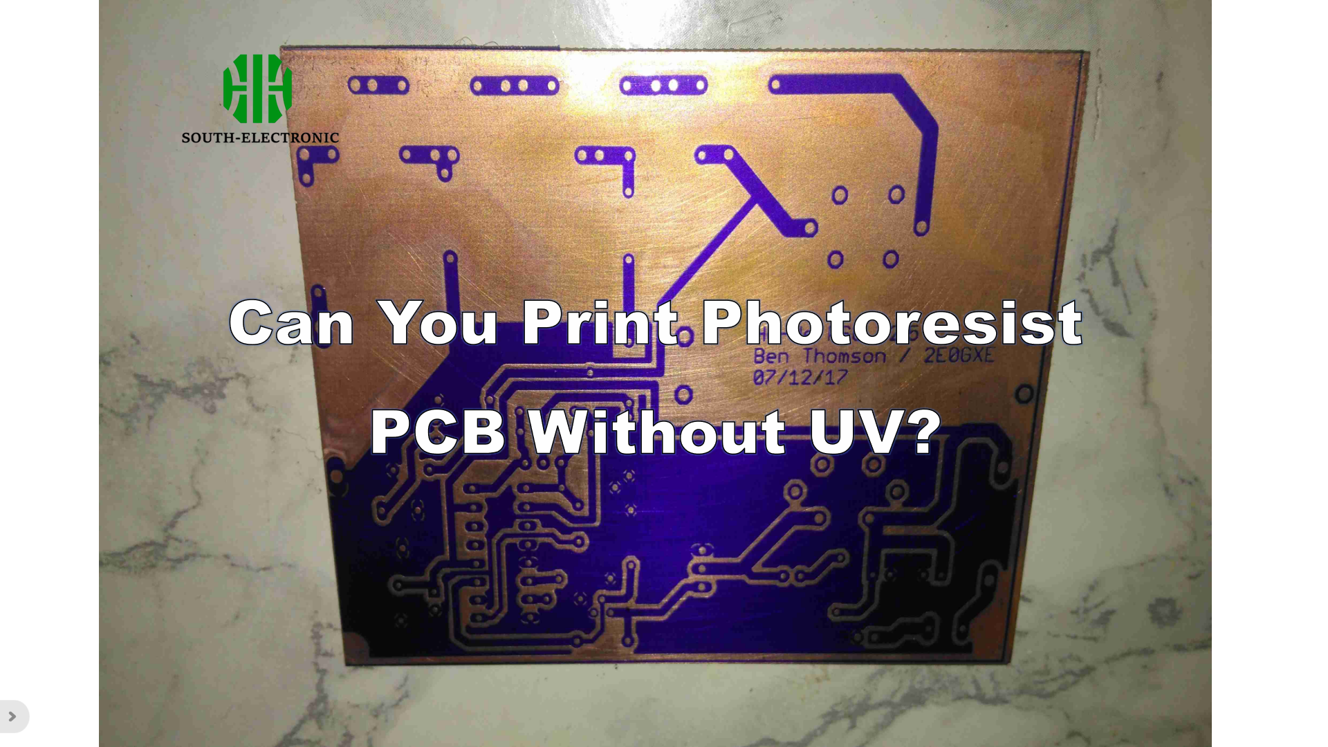
Can You Print Photoresist PCB Without UV?
The traditional method of printing PCBs involves using UV light to cure the photoresist, a light-sensitive material. But what if you don’t have access to a UV light source? Can you still print a photoresist PCB without UV? Yes, you can. UV cure ink is not the only type of ink available for PCB solder masks.
Why Consider Alternatives to UV?
In the world of PCB manufacturing, photoresist is a material that is sensitive to light, typically ultraviolet (UV). When exposed to UV light, the photoresist undergoes a chemical change that allows it to either harden or soften, depending on the type of photoresist used (positive or negative). This process is crucial for creating the intricate patterns needed for circuit boards.
While UV-based methods are popular due to their precision, they aren’t always accessible. UV lamps and exposure units can be expensive and require careful handling. For hobbyists, students, and even some professionals, finding alternative methods can make PCB manufacturing more accessible and cost-effective.
Alternative Methods for Printing Photoresist PCBs
There are several methods to print photoresist PCBs without using UV light. These methods vary in complexity, cost, and the quality of the final product. Below, we explore these methods in detail.
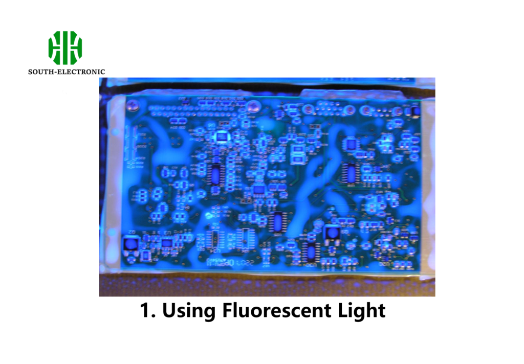
1. Using Fluorescent Light
Fluorescent lights are a common household item that can be repurposed for PCB manufacturing. They emit light that, while not as intense as UV, can still expose certain types of photoresist.
Pros:
- Accessibility: Fluorescent lights are widely available.
- Cost-effective: Lower cost compared to UV exposure units.
Cons:
- Longer Exposure Time: The exposure time required is significantly longer than UV methods.
- Inconsistent Results: The light intensity and wavelength may not be consistent, leading to variable results.
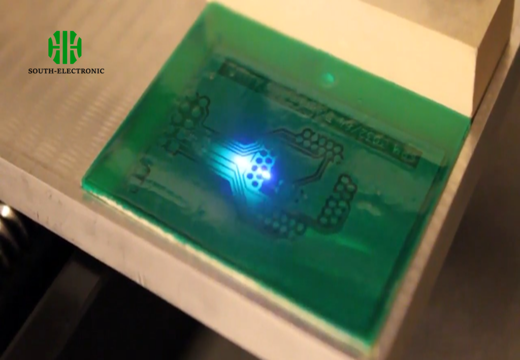
2. Using Laser Printers for Direct Printing
Another method involves using laser printers to print the PCB pattern directly onto the photoresist. This method is known as toner transfer and can be quite effective.
Pros:
- Precision: Laser printers can produce high-resolution patterns.
- No Special Equipment Required: No need for light sources or exposure units.
Cons:
- Limited to Certain Photoresists: Not all photoresists are compatible with this method.
- Requires a Special Paper: Toner transfer paper is necessary for this method.

Comparison with UV Method
Each method has its advantages and disadvantages when compared to the traditional UV method. Below is a comparison table that highlights key aspects.
| Aspect | UV Method | Fluorescent Light Method | Laser Printer Method |
|---|---|---|---|
| Precision | High | Moderate | High |
| Cost | High (for equipment) | Low | Moderate |
| Ease of Use | Requires specialized equipment | Simple setup | Requires a laser printer and transfer paper |
| Exposure Time | Short (minutes) | Long (20-30 minutes) | No exposure required |
How Long Do You Have to Expose the Photoresist Board to UV Light?
With UV light, a typical exposure time is around 1 minute. This is much faster than non-UV methods, but requires access to specialized equipment.
What is the Wavelength of Photoresist in PCB?
Photoresist materials used in PCB manufacturing are typically sensitive to UV radiation in the range of 300 nm to 440 nm. However, alternative methods bypass the need for UV light altogether.
How to Make a Photosensitive PCB?
Making a photosensitive PCB involves applying a light-sensitive photoresist to a copper board, exposing it to light through a patterned transparency, developing the exposed board, and then etching away the unprotected copper.
In conclusion, while the UV method for printing photoresist PCBs is efficient and widely used, it is not the only option available. Fluorescent light and laser printer methods offer viable alternatives, especially for those without access to UV equipment. These methods, though varying in complexity and precision, make PCB manufacturing accessible to a broader audience.

