
What is via filling?
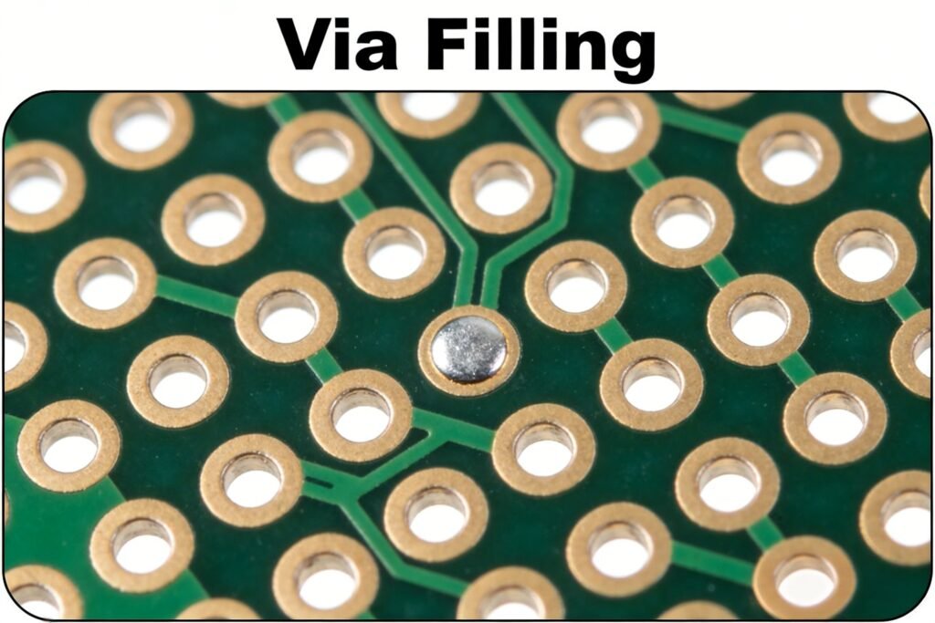
Via filling improves PCB reliability by fully filling plated through-holes, preventing issues like air/moisture entrapment.
Why is a solder bridge a serious problem for your electronics?
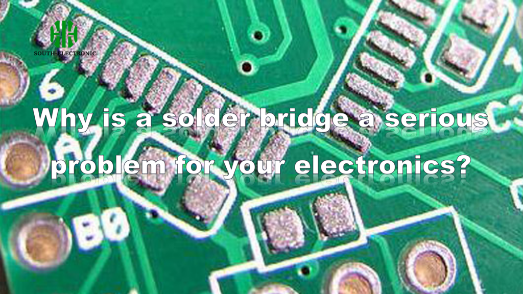
Prevent catastrophic PCB failures: Learn critical solder bridge avoidance strategies in design spacing, solder mask barriers, reflow controls, and AOI inspection to save costs.
My PCB is Warped! Can I Fix It?
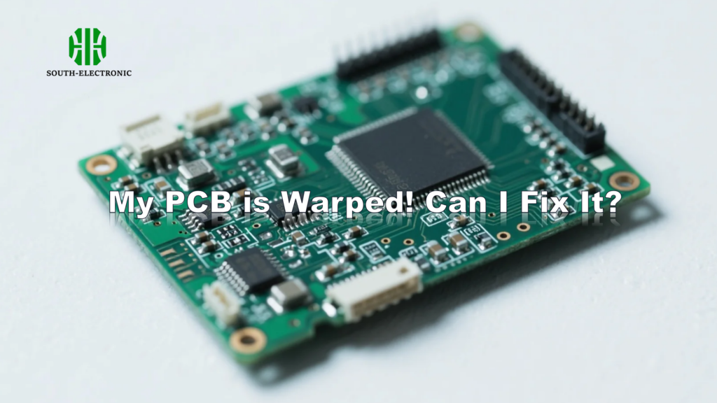
My PCB warped overnight! Assembly lines halted because bent boards won’t solder. Your profits vanish when warped PCBs fail. I found that quick action might save some boards. Mild warpage can be fixed with controlled heating, but severe cases need total replacement. Heat treatment reshapes mildly bent boards by relaxing internal stress inside the PCB […]
What Are the Most Common Causes of PCB Failure?
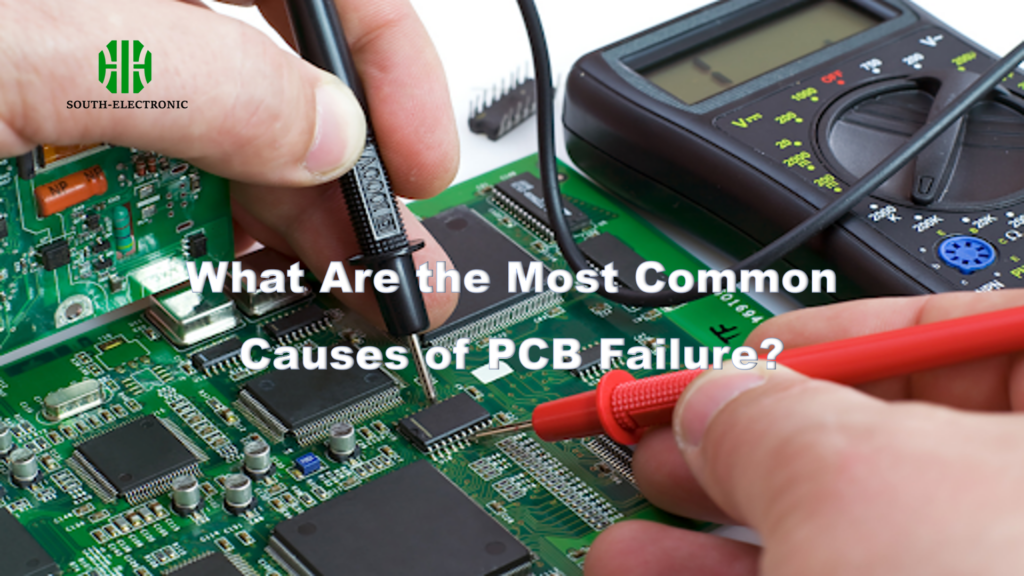
Diagnose & prevent common PCB failures: manufacturing flaws, environmental stress, soldering defects. Learn visual inspection, repair techniques & cost-effective solutions.
What is a Short Circuit?
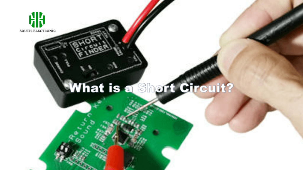
Discover why short circuits spark deadly fires, how to detect hidden electrical faults, and crucial steps to prevent disaster. Stay safe with expert insights.
PCB Tombstone: What Is It and How to Avoid It?
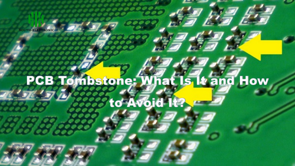
Prevent PCB tombstoning via balanced pad design, precise thermal profiles, and controlled solder paste to neutralize uneven solder forces.
Open Circuit vs Short Circuit: How Do We Fix It?
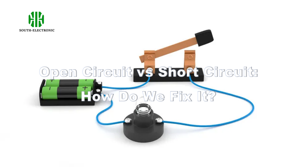
Spot open vs short circuits: visual signs, safe repairs, smart prevention. Electrician insights to prevent fires and fix electrical issues.
How to Design ESD Protection Circuit for PCBs?
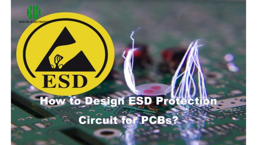
Master ESD protection with strategic component selection, optimized PCB layouts, and rigorous testing to prevent static-induced electronics failures.
What’s the Difference between EMI, EMS and EMC?
Master EMI control, EMS resilience & EMC compliance for robust IoT/5G devices. Essential design practices to eliminate electromagnetic failures
How to Optimize PCB Wiring for High-Speed Circuits?
Master high-speed PCB design with impedance control, differential routing, and EMI-reducing stackups to prevent signal loss and ensure compliance.
