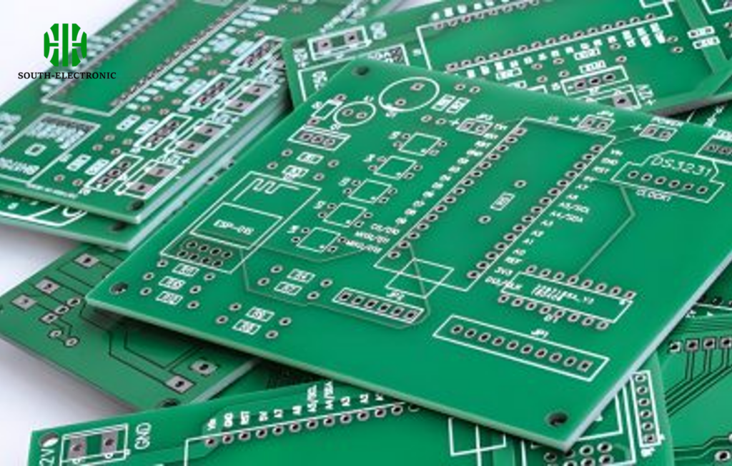
What is Prepreg vs Core?

Understand PCB core (rigid copper backbone) vs. prepreg (bonding adhesive). Correct prepreg selection prevents delamination, signal loss, and thermal failures in multilayer boards.
Which is the most popular PCB design software?
Compare top PCB tools: Altium for complex designs, Eagle for teams/hobbyists, KiCad for free open-source. Avoid AutoCAD for electronics. Cloud collaboration tips & cost analysis included.
What are PCB post-drilling processes?
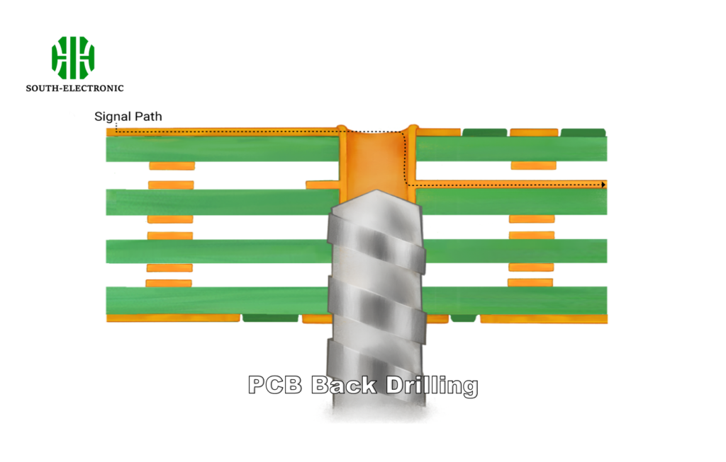
Master PCB drilling reliability by optimizing parameters, preventing defects like resin smear, and choosing mechanical/laser drilling based on hole specs for signal integrity.
How Do You Avoid Common Mistakes in Basic PCB Antenna Design?
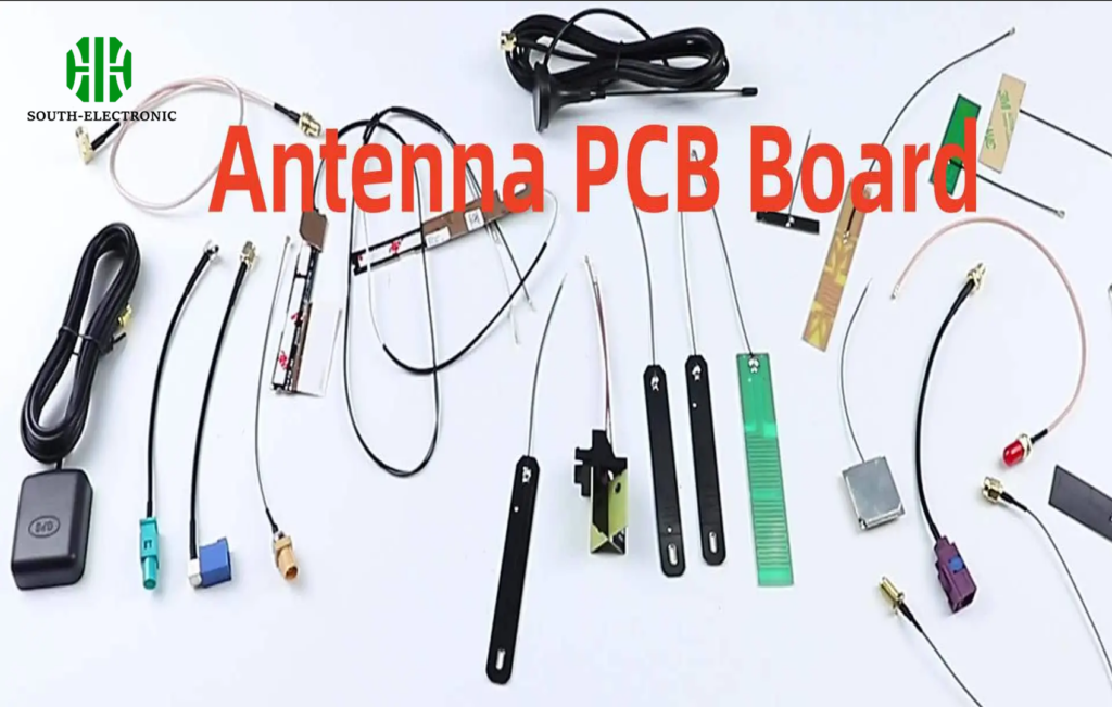
Prevent PCB antenna failures: optimize clearance, ground planes & simulations. Match antenna types to frequency, space & cost. Validate designs for robust wireless performance.
What certification requirements are required for PCB medical?
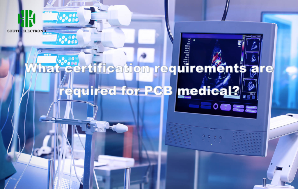
Medical PCB certifications (ISO 13485/IEC 60601) ensure safety. Strategies cut costs without sacrificing quality. Vetting suppliers is critical. Biodegradable/AI PCBs are the future. Patient safety depends on compliance.
What is the best PCB material for high-frequency?
Rogers, Isola, or Panasonic laminates outperform FR-4 for GHz circuits. Learn high-speed vs RF PCB differences, 5G signal loss fixes & best surface finishes for RF.
What is a probe test used for?
Unlock faster circuit diagnostics with probe testing. Compare flying probe vs. ICT methods, top systems (SPEA, Keysight), and optimize workflow duration for lower costs.
Where are BGAs used most?
Prevent PCB overheating: choose heatsinks by material/geometry, Optimize SMT stencil thickness (0.1-0.2mm), design apertures to prevent bridges, apply coatings for fine-pitch components, and maintain stencils to extend lifespan for flawless solder paste deposition.
What are the different types of PCB surface finishing?

Choose the right PCB surface finish to avoid solder failures: HASL for low-cost prototypes, OSP for quick assembly, ENIG/ENEPIG for RF/high-reliability. Balance cost, signal needs, and lead time.
What Standards Define Quality & Compliance in Medical PCB Assembly?
Medical PCB lives depend on IPC Class 3, ISO 13485 & FDA compliance. Prevent failures: learn material requirements, cleanroom protocols & vital supplier certifications for lifesaving devices.