
The complexity of electronic designs has led to a growing need for multilayer PCBs (Printed Circuit Boards). These intricate boards offer higher density and more compact solutions for modern electronics, making them essential in many applications. However, multilayer PCB fabrication is complex and usually requires specialized equipment, particularly for lamination under high pressure and temperature. Despite these challenges, with a little creativity and careful planning, you can attempt some DIY methods to produce simpler multilayer PCBs at home.
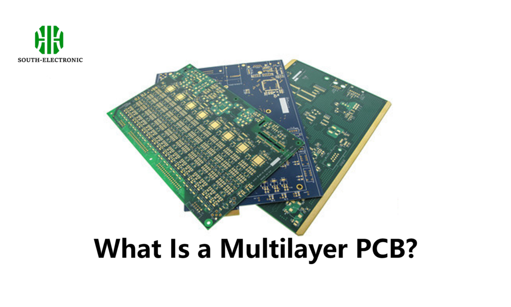
What Is a Multilayer PCB and Why Is It Challenging to Fabricate?
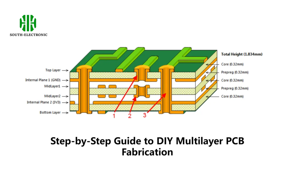
A multilayer PCB is a printed circuit board with more than two layers of conductive copper. Unlike single-layer and double-layer PCBs, multilayer PCBs have multiple layers of copper separated by insulating layers, all laminated together to form a single board. These boards are used in advanced electronics like smartphones, computers, and medical devices because they offer greater flexibility, higher component density, and better performance.
Challenges in Multilayer PCB Fabrication
- Layer Alignment: Ensuring that all layers are perfectly aligned is critical to the PCB’s functionality.
- Lamination: The layers must be bonded together under high pressure and temperature, which typically requires specialized industrial equipment.
- Through-hole Plating: Creating electrical connections between layers often involves electroplating, which is difficult to achieve in a DIY setting.
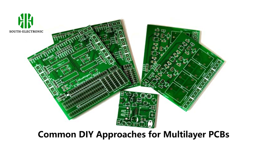
Common DIY Approaches for Multilayer PCBs
Making professional-grade multilayer PCBs at home is hard, but you can make simpler versions using some DIY methods.
1. Stacking Single-layer Boards
One of the simplest methods involves stacking several single-layer PCBs together and using adhesives to bond them. This method, while not as reliable as professional fabrication, can be useful for prototypes or low-cost projects.
2. Using Thin Blanks and Adhesives
Another approach is to use thin copper-clad blanks that can be laminated together using strong adhesives. This method requires careful alignment and a steady hand but can produce reasonable results for non-critical applications.
3. Creative Lamination Techniques
Some hobbyists have experimented with using vacuum bags and homemade presses to apply the necessary pressure for lamination. While these methods are far from perfect, they can work for small-scale, low-frequency circuits.
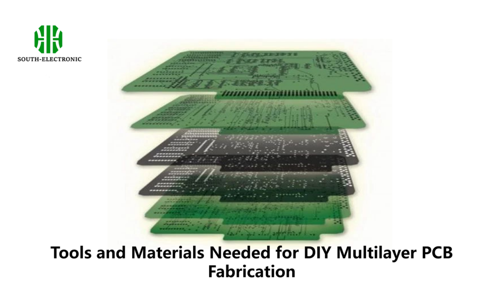
Tools and Materials Needed for DIY Multilayer PCB Fabrication
Creating multilayer PCBs at home requires specific tools and materials. Below is a table summarizing the essentials:
| Tool/Material | Purpose |
|---|---|
| Copper-clad Laminates | Base material for each PCB layer |
| Epoxy Adhesives | Bonding layers together |
| Alignment Pins | Ensuring precise layer alignment |
| Etching Chemicals | Removing unwanted copper from each layer |
| Drill Press | Creating vias and through-holes |
| Vacuum Bag or Homemade Press | Applying pressure during lamination |
Step-by-Step Guide to DIY Multilayer PCB Fabrication
Here’s a detailed guide to creating a simple multilayer PCB at home:
Step 1: Designing the PCB Layout
Start by designing your PCB layout using software like Eagle, KiCad, or Altium Designer. Ensure that your design accounts for all layers, including the internal connections.
Step 2: Preparing the Copper-clad Laminates
Cut the copper-clad laminates to the desired size. Clean the surfaces to remove any contaminants that could affect the adhesion of the layers.
Step 3: Etching the Copper Layers
Using etching chemicals, remove the unwanted copper from each laminate, leaving only the circuit traces. Ensure each layer is properly aligned with the others.
Step 4: Aligning the Layers
Use alignment pins or other tools to ensure that all layers are perfectly aligned. This step is crucial for the functionality of the final board.
Step 5: Laminating the Layers
Place the aligned layers in a vacuum bag or homemade press. Apply epoxy adhesive between each layer and press them together under high pressure. Let the assembly cure according to the adhesive manufacturer’s instructions.
Step 6: Drilling Vias and Through-holes
After the lamination process, use a drill press to create vias and through-holes for components and inter-layer connections.
Step 7: Plating Through-holes (Optional)
If through-hole connections are required, consider electroplating to ensure reliable electrical connections between layers. This step may be skipped for simpler designs where soldering is sufficient.
Potential Challenges and How to Overcome Them
1. Misalignment of Layers
One of the most common issues in DIY multilayer PCB fabrication is the misalignment of layers. This can lead to circuit failures and reduced reliability.
- Solution: Use alignment pins or professional-grade PCB alignment tools to minimize the risk of misalignment.
2. Air Bubbles During Lamination
Air bubbles trapped between layers can weaken the board and cause it to fail under stress.
- Solution: Ensure that the lamination process is conducted in a controlled environment, using a vacuum bag if possible, to remove any trapped air.
3. Poor Adhesion Between Layers
Inadequate bonding between layers can lead to delamination, especially under thermal or mechanical stress.
- Solution: Use high-quality epoxy adhesives and apply consistent pressure during the curing process.

What Are the Limitations of DIY Multilayer PCB Fabrication?
While DIY approaches can be used for prototyping or educational purposes, they come with significant limitations:
- Precision: Achieving the high precision required for complex multilayer PCBs is difficult without professional equipment.
- Layer Count: DIY methods are typically limited to 2-4 layers, whereas commercial PCBs can have up to 16 layers or more.
- Reliability: Homemade PCBs may not offer the same level of reliability, particularly in demanding applications.

