What is the Difference Between EDA and PCB?
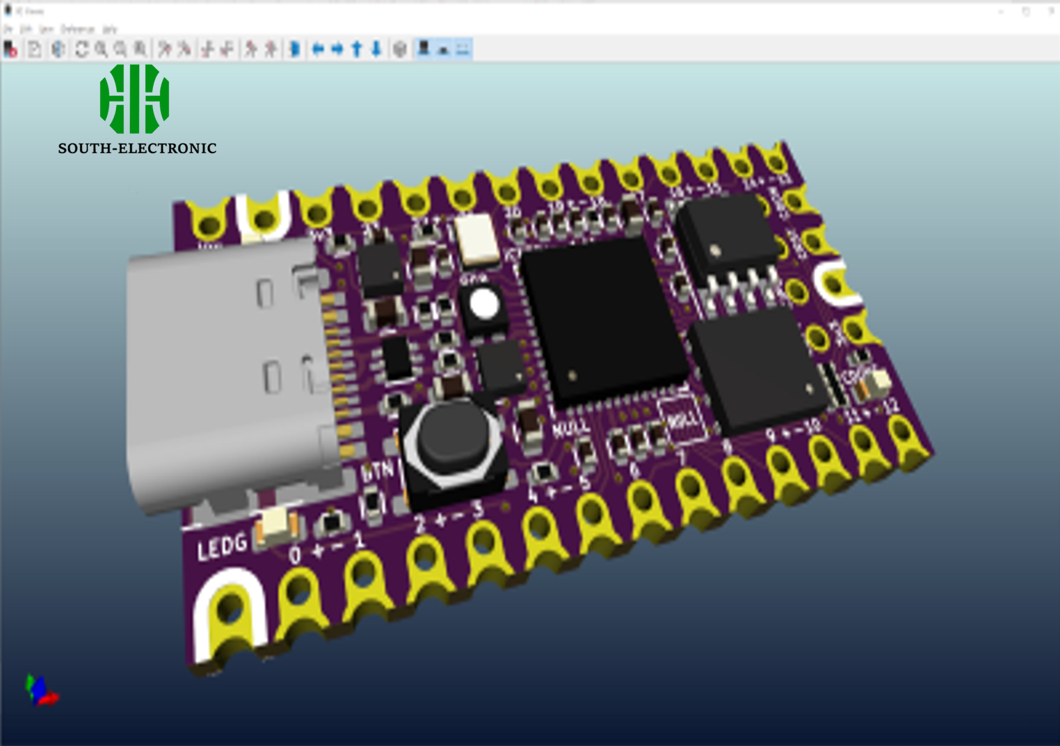
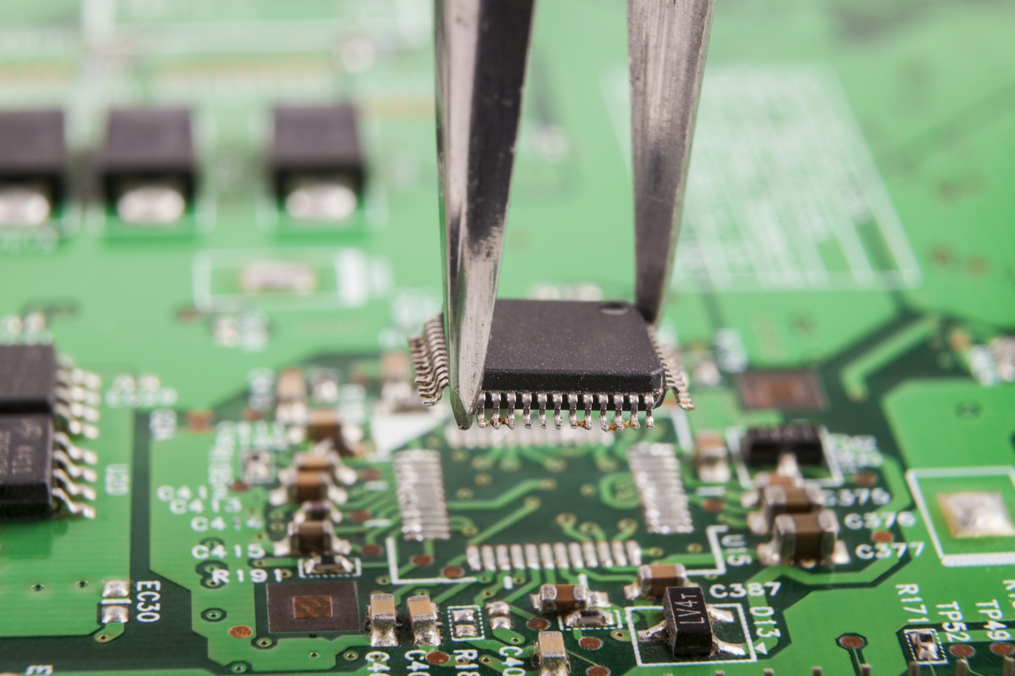
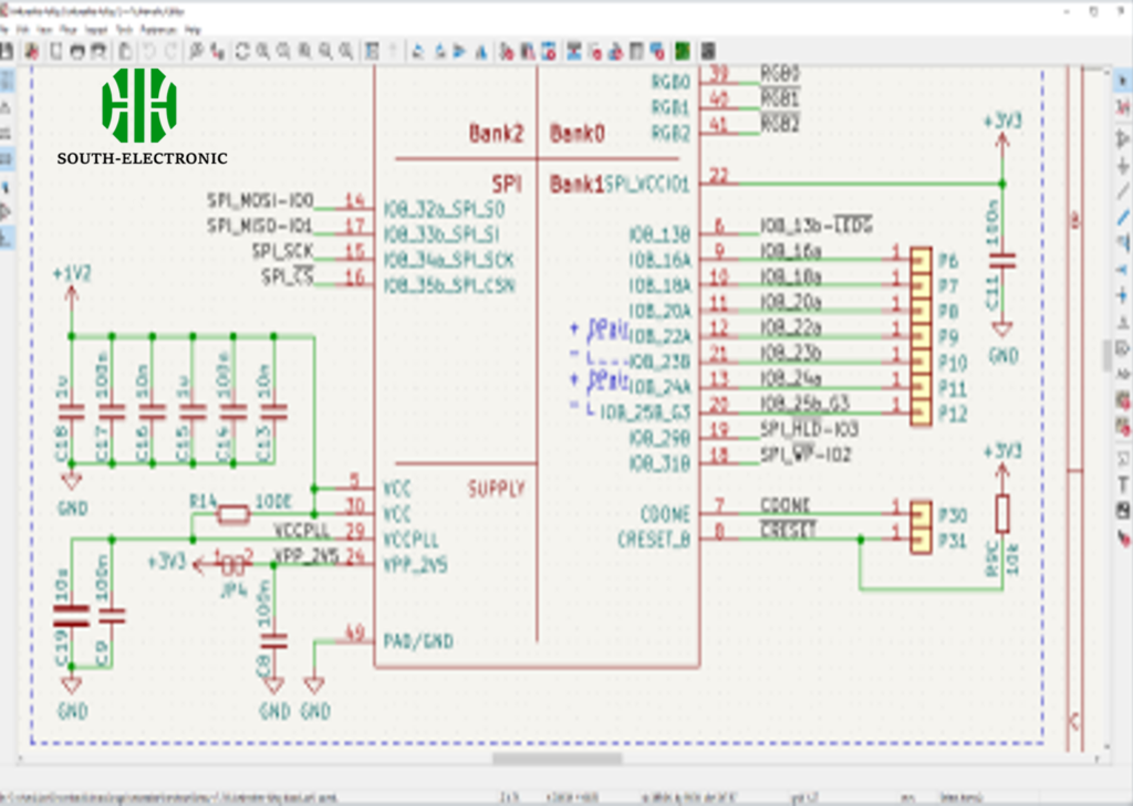
Electronic Design Automation (EDA) , short for Electronic Design Automation, is a type of software that people use to design electronic systems. These tools are super important for designing, simulating, verifying, and analyzing electronic circuits and systems. That includes things like integrated circuits (ICs) and printed circuit boards (PCBs). PCBs are the actual boards that hold electronic components and connect them electrically. EDA tools are a big deal when it comes to designing and developing PCBs. They make the design process faster, reduce mistakes, and make everything more efficient.
Key Functions of EDA Tools
- Schematic Capture: Allows designers to create circuit diagrams.
- Simulation and Verification: Provides the ability to simulate circuits and verify their functionality before physical production.
- Layout Design: Helps in designing the physical layout of ICs and PCBs.
- Testing and Analysis: Offers tools for testing and analyzing circuit performance under various conditions.
Examples of Popular EDA Software
- Altium Designer
- Eagle
- KiCad
- Cadence Allegro
- Mentor Graphics

What is PCB (Printed Circuit Board)?
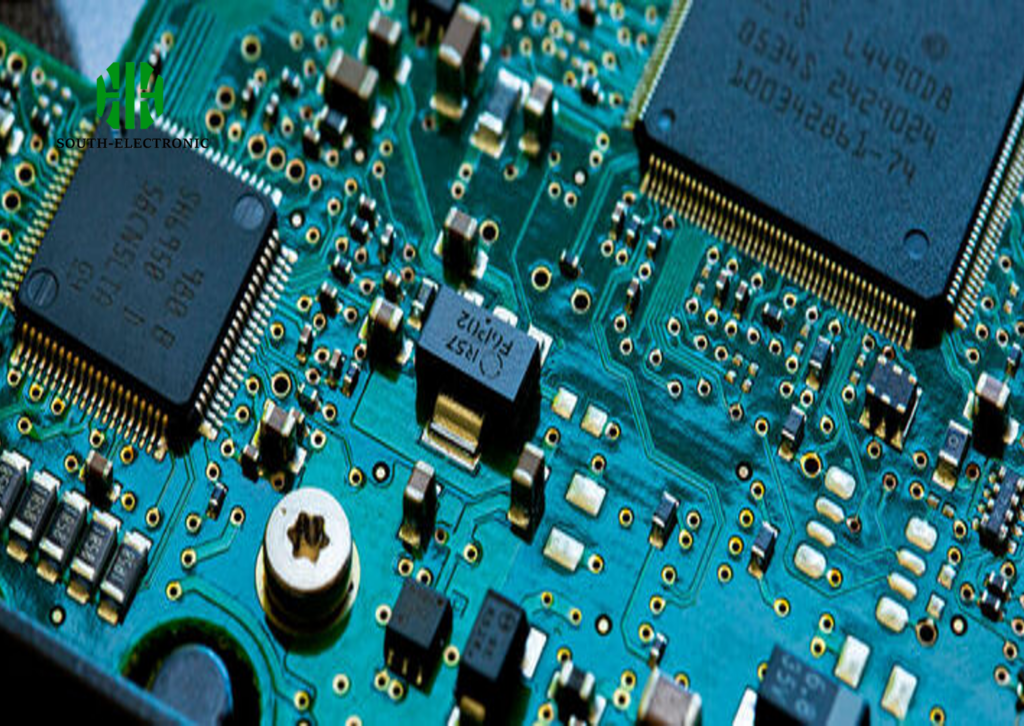
Printed Circuit Boards (PCBs) are the physical boards that house electronic components and provide electrical connections between them. PCBs are essential in virtually all electronic devices, from simple gadgets to complex industrial machines.
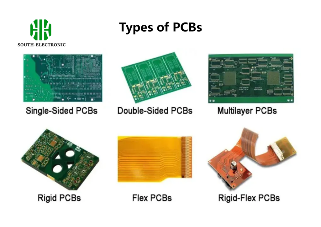
Types of PCBs
- Single-sided PCBs: Have components and copper tracks on one side only.
- Double-sided PCBs: Feature components and tracks on both sides.
- Multi-layer PCBs: Consist of multiple layers of substrate and circuits, offering complex interconnections.
Applications of PCBs
PCBs are used in various industries, including consumer electronics, automotive, aerospace, telecommunications, and medical devices.
Steps in PCB Design Using EDA Tools
- Schematic Capture: Creating a circuit diagram using EDA software.
- Component Placement: Arranging components on the PCB layout.
- Routing: Designing the pathways for electrical connections.
- Simulation and Verification: Testing the design for functionality and performance.
- Final Layout Design: Completing the physical layout for manufacturing.
Importance of Simulation and Testing:
Simulation and testing are crucial in the EDA process to ensure that the PCB design meets the required specifications and functions correctly under various conditions.
Differences Between EDA and PCB
Functional Differences
- EDA: Software tools used for designing and simulating electronic systems.
- PCB: The physical board where electronic components are mounted.
The Design Process vs. The Manufacturing Process
- EDA: Involves designing, simulating, and verifying circuits.
- PCB: Involves the physical production and assembly of the designed circuits.
Use Cases and Examples
- EDA: Used by designers and engineers to create and test circuit designs.
- PCB: Used in manufacturing to produce the actual electronic devices.
Comparison of EDA Software Tools
Here is a table comparing some popular EDA tools:
| Feature | Altium Designer | Eagle | KiCad | Cadence Allegro | Mentor Graphics |
|---|---|---|---|---|---|
| Schematic Capture | Yes | Yes | Yes | Yes | Yes |
| Simulation and Verification | Yes | Limited | Yes | Yes | Yes |
| Layout Design | Yes | Yes | Yes | Yes | Yes |
| User Interface | User-friendly | Moderate | Moderate | Advanced | Advanced |
| Price | High | Moderate | Free | High | High |

Real-World Examples and Case Studies
Example 1: Consumer Electronics Design
Designing a consumer electronics product using Altium Designer, from initial concept to final PCB production. This includes schematic capture, component placement, routing, and simulation.
Example 2: Open-Source Hardware Project
Using KiCad for an open-source hardware project, highlighting the benefits of free EDA tools. This showcases the complete design process and the final PCB implementation.

Future Trends in EDA and PCB Technology
Emerging Technologies in EDA
- AI and Machine Learning: Enhancing design automation and optimization.
- Cloud-based EDA: Offering collaborative design and simulation environments.
Advances in PCB Manufacturing Techniques
- Flexible PCBs: Enabling new applications and designs.
- High-density Interconnect (HDI) PCBs: Providing more connections in a smaller area.
Understanding the difference between EDA and PCB is crucial for anyone involved in electronics design and manufacturing. EDA tools are essential for designing and simulating electronic circuits, while PCBs are the physical boards that implement these designs. Both play a vital role in the creation of modern electronic devices.

