
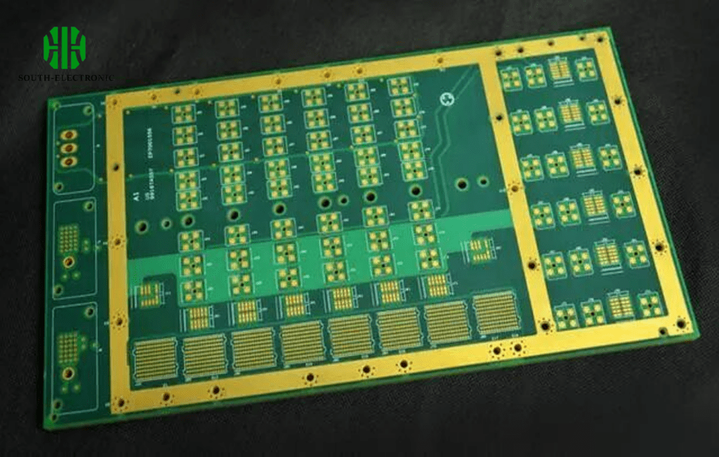
Ever ordered a custom PCB only to discover heat warping or signal interference? These common nightmares waste budgets and delay projects. Smart material choices prevent such disasters.
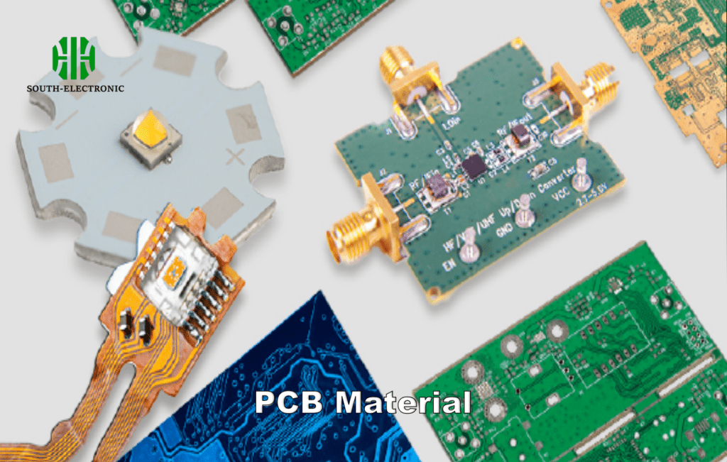
Focus on your project’s key needs first. Critical electrical factors include impedance control and signal integrity; thermal priorities involve Tg ratings and heat dissipation; mechanical/environmental demands cover flex requirements and operating conditions. Standard FR-4 fiberglass works for most boards, but high-frequency designs often need polyimide or ceramic.
Understanding materials is just your starting point. The real cost drivers, prototyping decisions, and supplier selection dramatically impact your custom PCB journey. Let’s examine these critical factors.
What factors affect custom PCB costs?
Watch your budget vanish when unexpected charges hit. Simple choices like board thickness or solder mask color can double expenses without warning.
Cost hinges on board complexity and material choices. Layer count impacts pricing most—each added layer increases cost by 15-30%. Material grade (standard FR-4 vs high-frequency laminates), surface finish quality, and hole density are major price drivers. Order quantity also shifts economics through volume discounts.
Decoding PCB Pricing Variables
Several interconnected elements determine your custom pcb price. Breaking them down helps optimize spending:
| Primary Factor | Cost Impact | Typical Range |
|---|---|---|
| Layer Count | Highest influence | 2-layer: $5-30 8-layer: $80-400+ |
| Base Material | Moderate to high | FR-4: Low Rogers: 3-5x FR-4 |
| Board Dimensions | Direct scaling | Below 100cm²: Low Above 500cm²: High markup |
| Special Features | Variable adder | Blind vias: +20% Gold plating: +35% |
Board size immediately affects raw material consumption. Larger formats waste more laminate during panelization and increase failure risks. For thermal/mechanical stability, thicker copper (over 2oz) adds copper etching costs. Minimum trace widths below 6 mil require advanced equipment, bumping up engineering fees. Volume breaks occur around 50 units, with over 500 pieces delivering 40%+ savings per board.
Is a custom PCB prototype necessary?
Skipping prototyping feels tempting to save time and custom pcb price. Until your full production run arrives with uncorrected design flaws that scrap the entire batch.
Prototypes are essential for functional validation and DFM checks. They catch 92% of design errors at 5-10% of mass production cost according to industry data. Exceptions: minor revisions of proven designs or ultra-low-cost disposable boards under $12.
When to Skip or Require Prototypes
Prototyping serves multiple risk-mitigation purposes:
| Prototype Type | Purpose | Cost Impact |
|---|---|---|
| Visual Mockup | Dimensional fit check | 3-5% of full run cost |
| Electrical Test Unit | Signal/power validation | 8-12% of lot value |
| Full Functional Prototype | Environmental & lifespan testing | 15-20% of project budget |
Simple Arduino shields might bypass prototypes if recycling known layouts—but any IoT product with RF components demands prototyping. High-layer-count boards (6+ layers) have alignment risks warranting test units. Work with your custom pcb maker to determine the right level: many offer discounted prototyping bundles that include design analysis. Online configurators help estimate this phase when considering custom pcb design online.
How to choose a reliable custom PCB supplier?
A supplier’s late delivery can freeze your production line. Worse—hidden quality flaws might cause product recalls months after shipment.
Vet potential suppliers through manufacturing audits and sample analysis. Critical benchmarks: IPC certification status, minimum order flexibility, DFM feedback quality, and testing documentation depth. Always request their data pack for a previous client project.
Supplier Selection Scorecard
Use this framework when comparing custom pcb designers:
| Evaluation Area | What to Verify | Red Flags |
|---|---|---|
| Technical Capability | Layer count limit Impedance control reports Material inventory | Single-process focus No test equipment photos |
| Quality Systems | ISO 9001 certification AQL sampling plans Cross-section reports | Vague inspection terms No quality documentation examples |
| Communication | Engineer response time ECN process clarity Design rule alerts | Generic quoting bots Unlisted phone support |
Prioritize suppliers offering online design rule checks through their custom pcb design software portal—it prevents manufacturing violations early. Smaller runs (under 50 units) suit custom pcb online services, but complex designs need experienced makers with in-house engineers. Ask for failure rate statistics: top suppliers maintain under 200 PPM defect rates. Always order sample boards before large commitments.
Conclusion
Selecting PCB materials requires understanding your project’s electrical, thermal, and mechanical needs. Balance costs with reliability, insist on prototypes for complex boards, and rigorously vet suppliers.
Want to make this process easier? South-Electronic has customized support that fits these needs.
With IPC certification and strict quality control (defect rate under 200 PPM), they’re a solid choice for turning your custom PCB design into a reliable product—perfect for projects dealing with tricky materials or budget limits.


