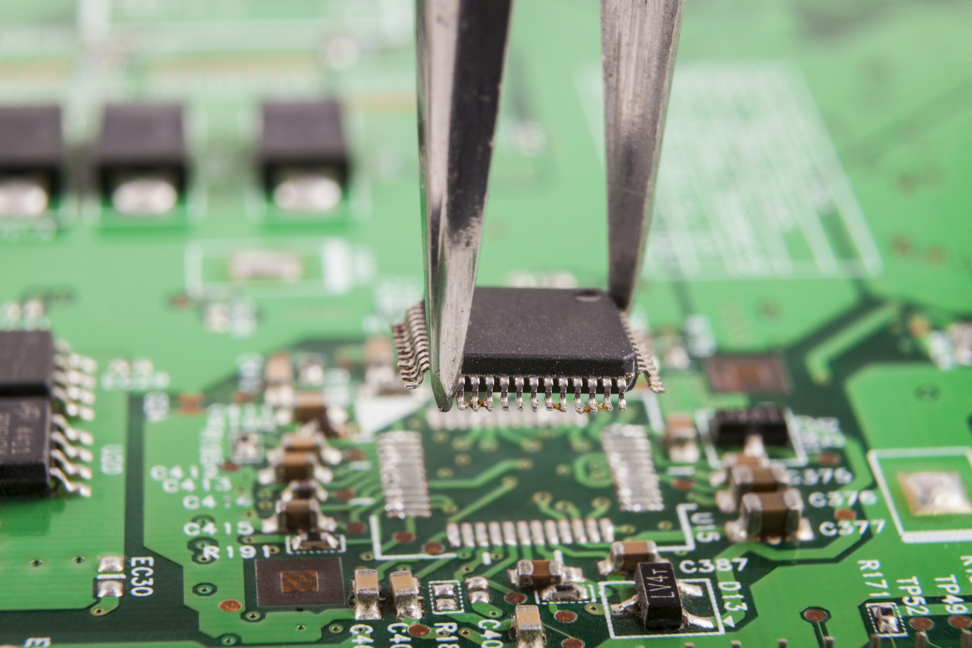
Ever spent hours debugging connections? Faulty PCB pins cause frustration. They lead to device failures. Your electronics deserve better. Choose wisely to avoid headaches.
Select pins based on three things. Match pin material to your environment. Ensure size fits both board and connector. Verify mechanical strength meets device stress. These prevent failures before your product ships.

Picking the wrong pin hurts your project. Mistakes cause big problems later. I learned this fixing industrial controllers. To avoid troubles, ask yourself four key questions.
Can PCB pin layout mistakes cause signal integrity issues?
Poorly placed pins ruin signal quality. I once saw interference crash sensors. This delayed our production line repairs.
Yes, messy layouts create three issues. Crosstalk mixes signals randomly. Impedance shifts break timing rules. Reflections make signals bounce back. Fix these by following spacing guidelines.

Fix layout mistakes using these rules
Bad layouts cause two types of signal damage. First, high-speed signals need clean paths. Noise creeps in with short spacing. Second, analog circuits fail with dirty routes. This happens near power lines.
| Problem Type | Cause | Fix |
|---|---|---|
| Crosstalk | Parallel traces 100 mil | Route equal-length traces with serpentines |
| Reflections | Impedance jumps at connectors | Use matching resistors at receiver end |
Digital systems need special care. Keep clock lines away from I/O pins. I solved timing errors this way. Also, ground planes protect sensitive analog signals. Add shielding around RF pins. Mechanical stress affects signals too. Use strain relief anchors near pins.
Why do PCB pins fail when soldered?
Soldering flaws kill pins silently. Our batch failed after thermal cycling. We found cold joints everywhere.
Three issues break solder bonds. Thermal shock cracks joints instantly. Contamination blocks solder flow. Wrong alloy causes premature fatigue.

Common soldering failures and solutions
Failed connections show clear patterns. Cold joints crumble under vibration. Thermal cracks spread over time. Contaminated pads reject solder completely.
| Failure Type | Warning Signs | Prevention |
|---|---|---|
| Cold solder | Dull surface, uneven shape | Preheat board, solder at 230-250°C |
| Thermal stress | Crack ring around pin | Match CTE, use flexible solder alloy |
| Solder skip | Bare copper visible | Clean with flux, control humidity during assembly |
I recall fixing test equipment failures. Always check solder temperature profiles. Use lead-free alloys for higher strength. Pins with plating last longer. Thin gold over nickel prevents oxidation.
How to test PCB pin durability?
Unseen wear causes field failures. Our outdoor sensors broke before warranty ended. Humidity attacks weak pins.
Test durability in three ways. Cycle pins 10,000+ times mechanically. Simulate temperature changes. Measure salt corrosion resistance.

Effective durability testing methods
Testing saves money after production. Mechanical stress shows weakness early. Environmental aging predicts field life well.
| Test Type | Equipment | Pass Standard |
|---|---|---|
| Insertion cycles | Force gauge jig | 4 weeks |
| Port access | Confirm shipping routes | No DDP incoterm |
Visit factories if possible. I saved costs with Shenzhen suppliers. Compare plating quality samples closely. Order trial batches first. Track shipping schedules daily.
Conclusion
Choose pins using electrical needs and environment tests. Match materials for your product life. Smart decisions create reliable connections every time.


