
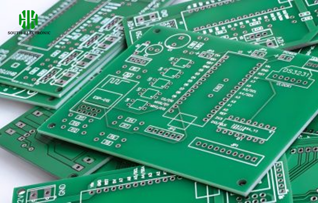
You sketch PCB concepts on paper but hit digital roadblocks. That exciting circuit stays trapped offline. Frustration builds as manufacturing needs Gerber files.
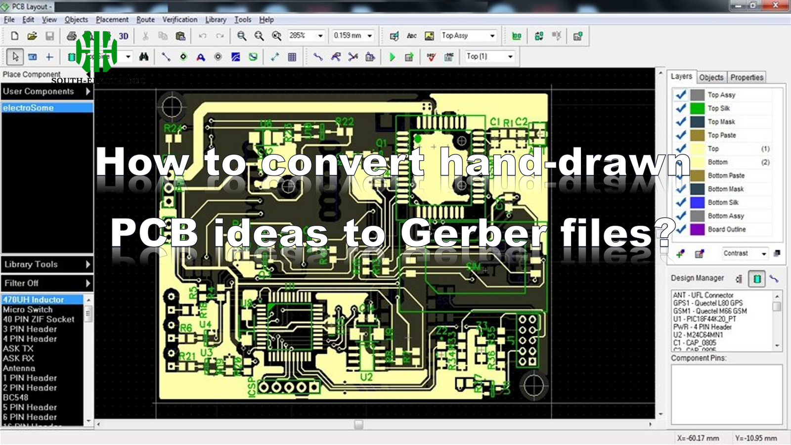
Converting hand-drawn PCBs requires recreating your sketch in Altium or Cadence software. Start by scanning drawings, then use built-in tools for precise digital tracing. Finally, generate Gerber files through the CAM processor. This process turns paper designs into manufacturable circuits.

Mastering this conversion unlocks manufacturing. Let me walk you through essential PCB drawing skills. We’ll tackle beginner steps, routing rules, and craft secrets.
Where should beginners start with PCB drawing in Altium/Cadence?
Hitting "New Project" overwhelms many novices. Blank screens paralyze progress when switching from paper.
Begin with scanning hand-drawn sketches directly into your PCB software. Use basic shapes like lines and pads to retrace components. Focus only on placement before complex routing. Both Altium and Cadence offer guided wizards for initial setup.
Core first steps breakdown
New users commonly struggle with three fundamental tasks. Follow this sequence:
| Task | Altium Method | Cadence Method | Time Saving Tip |
|---|---|---|---|
| Importing Sketches | Place > Drawing Tools > Line | File > Import > DXF | Use scanner at 300dpi minimum |
| Component Placement | Drag from Libraries panel | QuickPlace tool | Group related parts first |
| Board Outline Setup | Design > Board Shape | Setup > Outlines > Board | Match paper dimensions exactly |
Start by recreating your paper sketch digitally without wires. Component positioning comes first. Both tools have library managers—place resistors, ICs, and connectors where drawn. Ignore routing completely at this stage. Set board edges using the line tool, tracing your paper border. This foundation prevents redesign chaos later.
What are the best practices for PCB drawing?
Ever get buzzing circuits or signal ghosts? Random wiring causes most noise issues.
Always separate power and signal paths during routing. Maintain clearance gaps between traces. Use ground planes liberally under noisy components.

Layout strategy fundamentals
These practices prevent common circuit failures:
Power routing principles
- Use star topology for power distribution
- Keep supply traces short and thick
- Place decoupling capacitors near IC power pins
Signal integrity rules
- Avoid 90-degree trace angles
- Route differential pairs parallel
- Match trace lengths for timing signals
Noise containment tactics
- Implement ground pour on empty layers
- Shield clocks with ground guards
- Group analog/digital sections separately
Apply these during digital tracing in your software. Set design rule checks (DRC) before routing: minimum clearance 0.2mm, trace width 0.3mm for signals. Route power lines first with wider paths. Remember ground return paths—unclosed loops create antennas. Critical signals go shortest routes. These techniques solve hand-drawn limitations.
Where do circuit design and visual creativity meet in PCB drawing?
Your PCB hides artistic potential beyond wiring. Functional circuits can also dazzle eyes.
Creative component arrangement tells visual stories through copper. Shapes and silkscreen become design elements while maintaining electrical soundness.
Merging aesthetics function
Circuit personality emerges through three techniques:
Shape-driven layouts
- Curve traces for fluid appearance
- Align components along non-grid patterns
- Design custom board outlines like gears
Strategic copper expression
- Use ground planes as negative space art
- Form logos with exposed pads
- Create thematic solder mask cutouts
Silkscreen storytelling
- Add component legends with playful fonts
- Illustrate signal flow with arrows
- Hide Easter eggs in component labels
I transformed a music amplifier into guitar-shaped PCB art. All while keeping impedance-controlled paths—creative layouts demand planning. Sketch concept art first! Separate high-current zones from sensitive audio inputs visually. Balance becomes key. Beauty in circuit design isn’t random but planned harmony.
Conclusion
Scan hand-drawn PCBs into Altium/Cadence carefully. Apply routing rules during digital recreation. Blend artistry with engineering for memorable boards. Manufacture creativity.

