
How to Improve the PCB Layout Level?
Improving the PCB layout is crucial for creating reliable, efficient, and cost-effective electronic devices. Whether you’re an electronics engineer, a hobbyist, or a student, optimizing your PCB layout can significantly impact your project’s success. In this comprehensive guide, we will explore various strategies and best practices to elevate your PCB design to the next level.
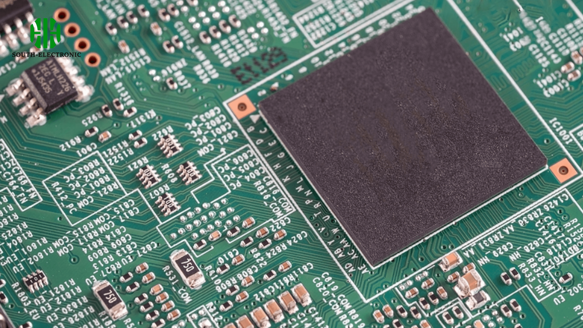
Get Better at PCB Layout
- Use Correct Grid Spacing: Maintain a consistent grid spacing throughout your design to avoid misalignment and routing issues.
- Avoid Multiple Grids: Stick to a single grid system to streamline the design process and reduce errors.
- Keep Traces Short and Direct: Minimize the length of signal paths to reduce noise and potential interference.
- Power Distribution: Ensure proper power distribution to prevent voltage drops and power integrity issues.
- Component Groupings: Group related components together to simplify routing and testing.
- Design Rule Check (DRC): Regularly perform DRCs to identify and fix design errors early.
- Use Silkscreens: Utilize silkscreens effectively for labeling and instructions on the PCB.

What Are the Considerations of PCB Layout?
| Consideration | Description |
|---|---|
| Component Placement | Logical arrangement to minimize signal path lengths. |
| Signal Integrity | Techniques to maintain signal quality and reduce noise. |
| Thermal Management | Strategies to dissipate heat and prevent overheating. |
| Electromagnetic Interference (EMI) | Methods to reduce EMI and protect components. |
What Are the Guidelines for PCB Layout?
- Planning Your Stack-Up:Start by planning the stack-up, which includes the arrangement of layers in the PCB. This helps in managing signal integrity and thermal performance.
- Setting Design Rules:Define design rules such as trace width, spacing, and via sizes. Adhering to these rules ensures manufacturability and reliability.
- Drawing the Board Outline:Create a precise outline of the PCB, considering mechanical constraints and mounting requirements.
- Component Placement:Place components strategically, considering signal flow and minimizing interference.
- Routing the Board Nets:Connect components with traces, ensuring short and direct paths. Use techniques like differential pairs for high-speed signals.
- Performing Design Rule Check (DRC):Regularly perform DRCs to catch errors early and ensure compliance with design rules.
- Completing PCB Fab/Assembly Notes:Document all necessary information for fabrication and assembly, including layer stack-up, drill files, and assembly drawings.
Table of Design Tools

Create a table listing popular PCB design tools, their features, and their use cases to help readers choose the right tool for their needs.
| Tool | Features | Use Case |
|---|---|---|
| Altium Designer | Advanced design and simulation tools | Professional PCB design |
| KiCad | Open-source, customizable | Hobbyist and educational projects |
| Eagle | User-friendly, integrated with Fusion 360 | Small to medium-sized projects |
| OrCAD | Robust simulation and analysis | Complex and high-performance PCBs |
Improving your PCB layout level involves a combination of strategic planning, adherence to design rules, and continuous learning. By focusing on component placement, signal integrity, thermal management, and EMI reduction, you can create efficient and reliable PCBs. For those new to PCB design, start with simple projects and gradually move to more complex designs. Utilize online resources, tutorials, and community forums to enhance your skills and knowledge.

