

What is a High-speed PCB?
A high-speed PCB is one that operates with signal speeds high enough to be affected by the physical properties of the board materials, layout, and environment. This usually refers to signal frequencies from the upper MHz to GHz range, where considerations like signal reflection, crosstalk, and electromagnetic interference (EMI) become significant factors in circuit design. These boards are commonly used in advanced communication systems, high-performance computers, and sophisticated consumer electronics.
How to Design a PCB for High-Speed PCB?
Designing a high-speed PCB requires careful consideration of both electrical and mechanical parameters to ensure signal integrity and system reliability. Here are some key steps in the design process:
- Material Selection: Choose substrate materials with low dielectric losses and stable dielectric constants, such as FR-4 or advanced materials like Rogers for extremely high-speed applications.
- Impedance Control: Design the trace geometry and stack-up to achieve the required impedance characteristics, ensuring consistent signal integrity.
- Signal Routing Guidelines: Route high-speed signals using the shortest and most direct paths possible. Avoid sharp bends and use differential signaling where feasible to minimize crosstalk and EMI.
- Use of Vias: Minimize the use of vias on high-speed signal paths, as they can introduce impedance discontinuities and potential reflections.
- Decoupling Capacitors: Place these near power pins of active components to stabilize power distribution and reduce noise.
- Thermal Management: High-speed components can generate significant heat, so ensure adequate cooling via heat sinks, thermal vias, and proper airflow.
- Testing and Validation: Use tools like time-domain reflectometry (TDR) to measure impedance and ensure the board meets design specifications.
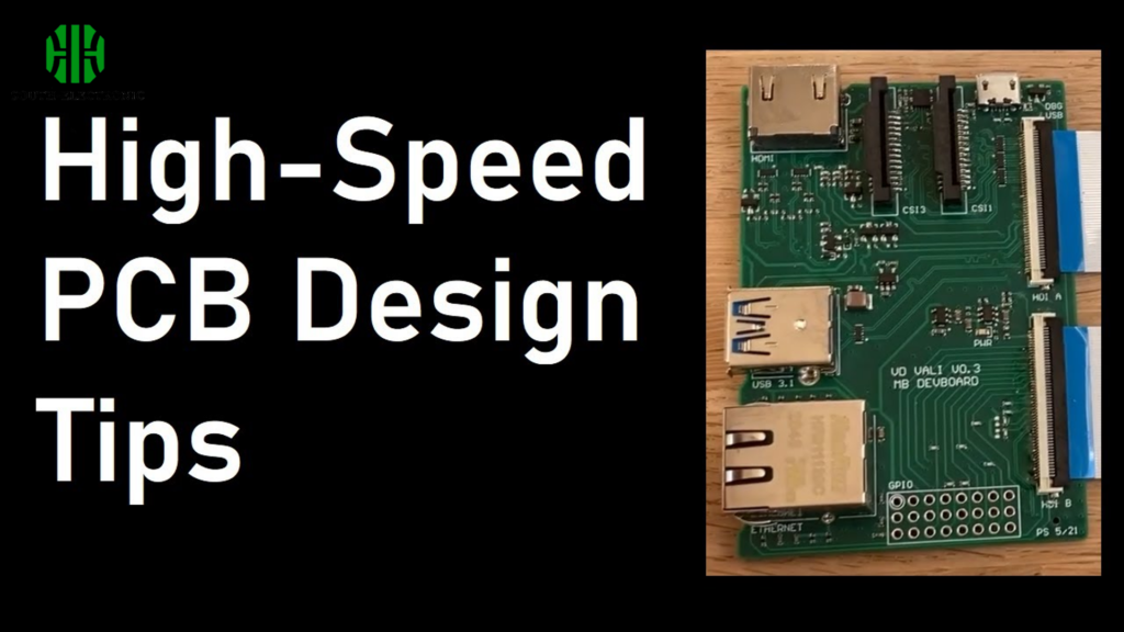
High-Speed PCB design Tips
- Maintain Consistent Trace Widths: This helps in managing impedance and minimizing signal loss.
- Avoid Parallel Routing: To reduce crosstalk, route high-speed traces perpendicular to each other when crossing is unavoidable.
- Use Ground Planes: These help in reducing EMI by providing a shield and reducing loop area.
- Keep Critical Signal Paths Short and Direct: This reduces the chance of signal degradation due to attenuation and dispersion.
- Consider the Effects of PCB Layout Early: Placement and routing should be considered in the initial stages to optimize performance.
What is the Best Material for PCB Design High-speed?
The best material for high-speed PCB design largely depends on specific application requirements such as frequency and thermal demands. FR-4 is cost-effective and suitable for lower-frequency high-speed applications, while advanced materials like Rogers, Megtron 6, and Isola provide superior performance for higher frequencies and critical operations due to their low dielectric losses and stable dielectric constants. Rogers materials are excellent for RF and microwave applications, Megtron 6 is ideal for high-speed data transmission, and Isola’s offerings cater to high-end computing and aerospace with high reliability. For the most cutting-edge high-speed digital applications, Tachyon® 100G offers specialized low loss characteristics perfect for high data rate systems, ensuring optimal signal integrity.
Challenges in Integrating High-Speed Serial Interfaces
- Signal Integrity: Maintaining high signal quality across connectors and cables can be challenging. This is often managed by ensuring controlled impedance and using quality connectors that match the signal requirements.
- EMI/EMC Compliance: High-speed signals can radiate significant electromagnetic interference, requiring careful layout, shielding, and grounding to meet regulatory standards.
- Power Integrity: Fluctuations and noise in the power supply can affect high-speed signal integrity. Using multiple layers of power planes and ample decoupling capacitors can help mitigate these effects.
- Physical Space Constraints: High-density interfaces may require more compact designs, which can be challenging to route without compromising performance.
Conclusion
High-speed PCB design is a complex engineering task that requires careful planning and precision across multiple stages—from selecting the right materials to optimizing the layout for signal integrity. By designing, testing, and validating with care, engineers can overcome the inherent challenges of high-speed PCB design, enabling advanced electronic systems that push the boundaries of technology.

