What are Mixed Signals in PCB?
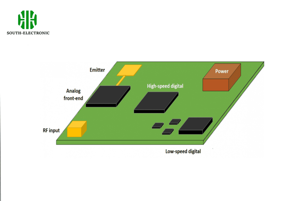
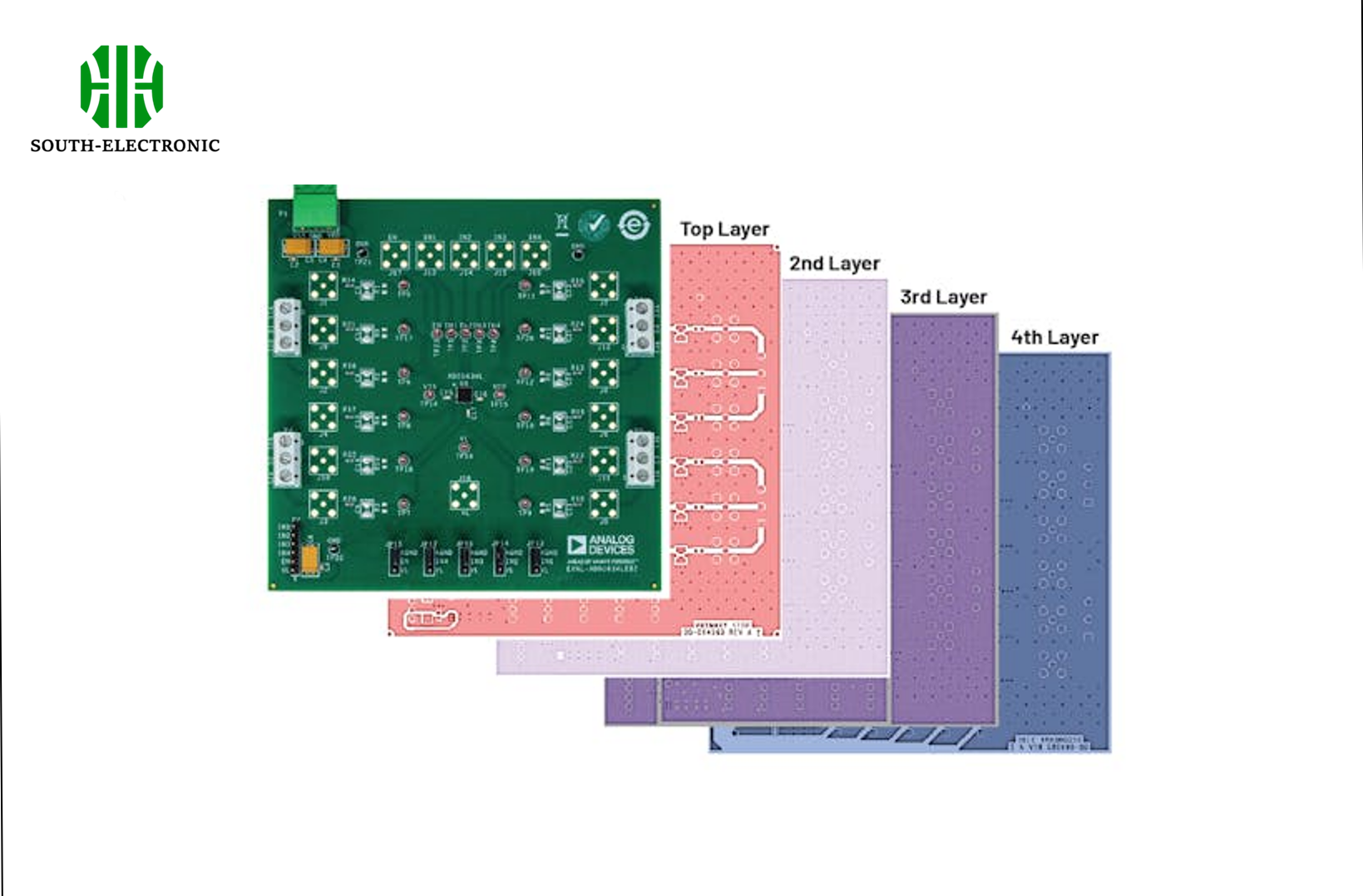
When we say “mixed signal,” we mean a combination of analog and digital signals in one system. A mixed signal PCB (Printed Circuit Board) is a type of circuit board that has both analog and digital circuits on it. A mixed signal PCB design is one that has both digital and analog circuits on it at the same time. To make these boards work right, you have to be careful about how you lay them out so you don’t get signal and power integrity problems.
What is a Mixed Signal PCB Design?
Key Design Strategies
- Partitioning: Separate analog and digital sections to minimize interference.
- Grounding Techniques: Use a unified ground plane with careful segmentation.
- Decoupling: Implement decoupling capacitors to filter noise.
| Component | Placement Area | Special Considerations |
|---|---|---|
| ADC | Analog Area | Isolate from digital components |
| DAC | Analog Area | Ensure proper grounding |
| FPGA | Digital Area | Use separate power plane |
| PLL | Analog Area | Shield to prevent interference |

What Software Tools Are Commonly Used for Mixed Signal PCB Design?
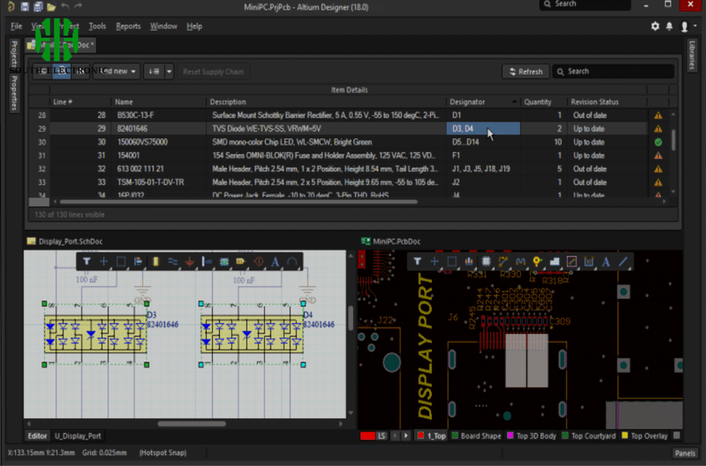
Commonly used software tools for mixed signal PCB design include Altium Designer, Cadence Allegro, Mentor Graphics PADS, OrCAD PCB Designer, Keysight ADS, and Proteus Design Suite.
- Altium Designer is known for its user-friendly interface and extensive libraries.
- Cadence Allegro offers robust design environments and powerful simulations.
- Mentor Graphics PADS provides integrated signal integrity and thermal analysis.
- OrCAD excels in schematic capture and detailed design rule checks.
- Keysight ADS specializes in RF and microwave circuit simulation.
- Proteus Design Suite is intuitive and strong in simulation, suitable for educational and small-scale projects.

How to Integrate RF Components in Mixed Signal PCBs?
- To integrate RF components in mixed signal PCBs, physically separate analog, digital, and RF sections to minimize interference.
- Use a continuous ground plane and isolate different sections’ grounds, connecting them at a single point.
- Ensure controlled impedance for RF traces, use metal shields for RF components, and place vias around RF traces.
- Provide separate power supplies for analog, digital, and RF sections with low-noise linear regulators, and place decoupling capacitors close to RF component power pins.
- Employ simulation tools for modeling and thoroughly test prototypes with spectrum and network analyzers for optimal performance.
When it comes to electronics, you gotta have a mixed signal PCB. It’s what lets you put digital and analog circuits together and make ’em work right. If you want your electronic devices to work the way they’re supposed to, you need to know what a mixed signal PCB is and how it works. That’s what I’m gonna tell you.


