
My PCB warped overnight! Assembly lines halted because bent boards won’t solder. Your profits vanish when warped PCBs fail. I found that quick action might save some boards.
Mild warpage can be fixed with controlled heating, but severe cases need total replacement. Heat treatment reshapes mildly bent boards by relaxing internal stress inside the PCB structure.
Let’s uncover why warpage happens and how to handle it. Critical PCB assembly questions follow now.
What’s the Maximum Allowable Warpage for Reliable PCB Assembly?
Warped PCBs ruin solder paste connections instantly. Your assembly line produces failures if warpage exceeds limits. I learned precise tolerances matter during my factory visits.
Standard IPC rules state 0.75% maximum warpage for reflow soldering. Manual assembly allows 1.5% for basic components. Beyond these limits causes open circuits or tombstoning issues.
Three Key Factors for Warpage Tolerance
We must review how applications and materials shape warpage limits. Tolerance depends on assembly methods and design complexity.
Component Size Impact
Tiny chips need tighter flatness because solder paste dots stay tiny. Larger components tolerate more bending without failures.
| Component Size | Max Warpage Tolerance |
|---|---|
| 0201 or smaller | 0.5% or less |
| Standard ICs | 0.75% |
| Connectors | 1.5% |
Thermal Profile Effects
Reflow oven heat worsens existing warpage by about 20% in my tests. Set your reflow settings carefully to avoid extra bending.
Material Choices
High-Tg laminates resist warpage better in hot reflow stages. Cheap FR-4 bends easily when temperatures exceed 150°C.
Always inspect boards before assembly starts. Measure warpage percentages at room temperature using proper tools.
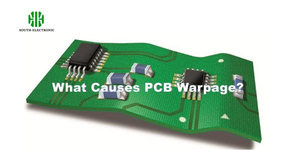
Which Materials and Processes Cause PCB Warpage?
Warpage wasted my early prototype batches constantly. Material reactions during manufacturing create internal board pulls. Your design choices trigger these common failure sources.
Copper layer imbalances and thin cores cause uneven tensions inside PCBs. Moisture absorption expands materials before reflow, creating permanent warpage after heating cycles.
Four Primary Warpage Origins
Understanding each cause helps prevent future damage. Material moisture and pressure errors dominate my failure logs.
Asymmetric Layer Stacks
I balance inner copper layers now. Having one thick layer on just one side bends boards during cooling.
Poor Lamination Control
Uneven heat or pressure in lamination machines causes internal stress. My worst case saw 2% warp from factory mishandling the platens.
Thermal Shock Damage
Rapid oven cooldown or uneven heating pulls boards unevenly. Allow slow cooling below Tg points, as sudden drops worsen distortions.
Moisture Swelling Issues
Storing PCBs in humid places adds hidden moisture that pushes layers apart when heated during assembly stages.
Pre-dry boards before reflow soldering if possible. Selecting symmetric designs and low-expansion laminates reduces risks significantly in your PCB processes.
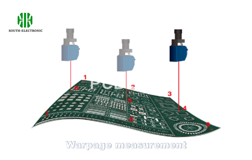
How Can I Accurately Measure PCB Warpage?
Guessing warpage visually causes costly rework mistakes. Your hand-towel method fails for tiny warps! Accurate data guides repair or replacement.
Laser scanners give digital warpage maps across entire PCB panels. I prefer shadow moiré testing because it reveals bend percentages at room temperature quickly.

Three Professional Measurement Systems
Each method fits different situations. I’ve tried all these systems during board failures and repairs.
Shadow Moiré Analysis
Projecting pattern distortions onto boards creates visual warp maps. I get percentage scores within 5 minutes using our inspection equipment. Works best during pre-assembly checks.
Coordinate Measurement Machines
CMM probes map hundreds of surface points precisely but slowly. I use these when diagnosing critical component placement issues manually on assemblies.
Laser Distance Scanners
Infrared lasers beam across boards to build 3D warp models. My fastest system gives reports showing warped zones requiring heat treatment.
| Method | Speed | Accuracy | Best Use Case |
|---|---|---|---|
| Shadow Moiré | Fast | Medium | Production Screening |
| Laser Scanner | Medium | High | R&D Analysis |
| CMM | Slow | Highest | Failure Diagnosis |
Place boards flat during testing and record measurements away from edges. Good data allows heat treatment decisions without process waste.
Conclusion
Fix mild PCB warpage with careful heating but replace bad cases. Prevent future warping by balancing materials and controlling moisture. Measuring accurately guides every repair choice.


