

Ever struggled with clunky wired connections in smart devices? NFC PCBs eliminate physical contact requirements while maintaining secure data flow. These intelligent circuit boards integrate wireless magic into compact spaces.
NFC PCBs[^1] embed near-field communication technology directly into printed circuit boards, enabling contactless data transfer[^2] and power exchange through precisely designed antenna coils and microchips – perfect for secure payment terminals and smart packaging solutions.
Let’s dissect how these wireless wonders transform traditional electronics through four critical aspects:
How Does NFC PCB Work?
Frustrated by limited connectivity in traditional circuits? NFC PCBs create invisible bridges between devices using electromagnetic fields. The process operates on resonant inductive coupling principles.
NFC PCBs communicate via 13.56MHz radio waves when devices come within 4cm range, using coiled antennas to generate magnetic fields that transfer both data and minimal power between chips.
)
Three-Stage Interaction Workflow
| Stage | Traditional PCB | NFC PCB |
|---|---|---|
| Initiation | Manual input required | Automatic handshake |
| Data Transfer | Wired connection | Magnetic field coupling |
| Power Source | External supply | Inductive energy harvesting |
The antenna coil’s geometry determines operational efficiency – tightly wound copper traces optimize field generation. During communication, initiator and target devices alternate between active (powered) and passive (field-powered) modes, enabling diverse applications from card emulation to peer-to-peer data sharing.
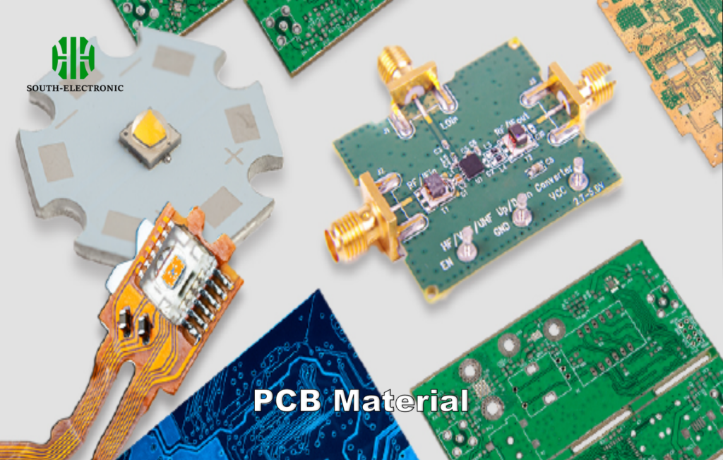
What Materials Are Used in NFC PCBs?
Why do some NFC boards fail in flexible wearables? Material selection dictates performance. Manufacturers balance electrical properties with mechanical constraints.
Key materials include FR-4 substrate[^3] for rigidity, polyimide[^4] for flexible designs, electroless nickel immersion gold (ENIG) plating[^5] for reliable contacts, and high-purity copper for antenna efficiency.
)
Material Performance Comparison
| Material | Key Property | Application |
|---|---|---|
| FR-4 Glass Epoxy | Stable dielectric constant (4.5-4.9) | Fixed-position antennas |
| Rogers RO3003 | Low loss tangent (0.0013) | High-frequency designs |
| Pyralux AP | 25μm adhesive layer | Flexible circuits |
| 2oz Copper | 70μm thickness | High-current antennas |
Copper thickness directly impacts antenna Q factor – thinner traces increase resistance but allow compact designs. Flexible substrates like polyimide endure >100k bending cycles while maintaining <5% impedance variation. Advanced manufacturers now experiment with silver nanoparticle inks for printed antennas in disposable applications.
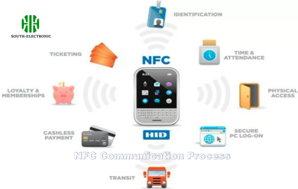
Where Are NFC PCBs Most Commonly Used?
From factory floors to retail checkouts, NFC solutions appear where reliability meets convenience. The technology's short range becomes an asset in secure environments.
Top applications include contactless payment terminals (42% market share), smart inventory tags (29%), medical device pairing (18%), and automotive keyless entry systems (11%).
)
Sector-Specific Implementations
| Industry | Use Case | NFC Advantage |
|---|---|---|
| Healthcare | Patient wristbands | HIPAA-compliant data access |
| Retail | Smart shelves | Real-time inventory updates |
| Automotive | Key fobs | Cryptographic authentication |
| Manufacturing | Equipment tracking | No-line-of-sight reading |
In pharmaceutical packaging, NFC chips store dosage history accessible through smartphone taps.[^6] Tesla's keycards use NFC PCBs with 128-bit encryption for vehicle access. Industrial implementations favor IP67-rated boards that withstand chemical exposure while maintaining stable RF performance.
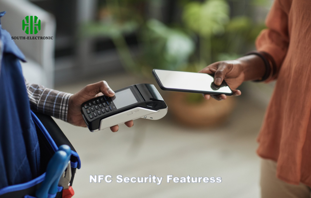
Are NFC PCBs Secure Enough for Payment Systems?
Payment fraud concerns haunt every new wireless tech. NFC's physical layer security provides inherent protection absent in Bluetooth/Wi-Fi systems.
NFC payments employ multiple safeguards: AES-128 encryption, single-use transaction codes, and physical proximity requirements that reduce remote hacking risks compared to other wireless protocols.
)
Security Architecture Layers
| Layer | Protection | Method |
|---|---|---|
| Physical | Limited range | 4cm operational boundary |
| Data | Encryption | AES/3DES algorithms |
| Protocol | Authentication | SAM modules |
| Application | Tokenization | Dynamic CVV |
EMVCo certifications require NFC payment PCBs to withstand 10kV ESD shocks and temperature extremes (-25°C to +70°C).[^7] Secure elements physically separate cryptographic operations from main processors. Dual-interface chips (contact + NFC) in credit cards use anti-tearing mechanisms to prevent data interception during transactions.
Conclusion
NFC PCBs revolutionize connectivity through secure, space-efficient wireless integration – from contactless payments to industrial IoT, proving that big innovations happen in close quarters.
[^1]: Explore this link to understand the technology behind NFC PCBs and their applications in modern electronics.
[^2]: Learn about the mechanisms of contactless data transfer, crucial for secure transactions and smart devices.
[^3]: Explore this link to understand the significance of FR-4 substrate in NFC PCB applications and its impact on performance.
[^4]: Learn about polyimide’s role in enhancing flexibility and durability in NFC PCBs, crucial for wearable technology.
[^5]: Discover how ENIG plating ensures reliable connections in NFC PCBs, vital for their performance and longevity.
[^6]: Discover how NFC technology is transforming pharmaceutical packaging and improving patient safety through easy access to dosage information.
[^7]: Exploring EMVCo certifications will provide insights into the rigorous standards ensuring NFC payment security and reliability.

