
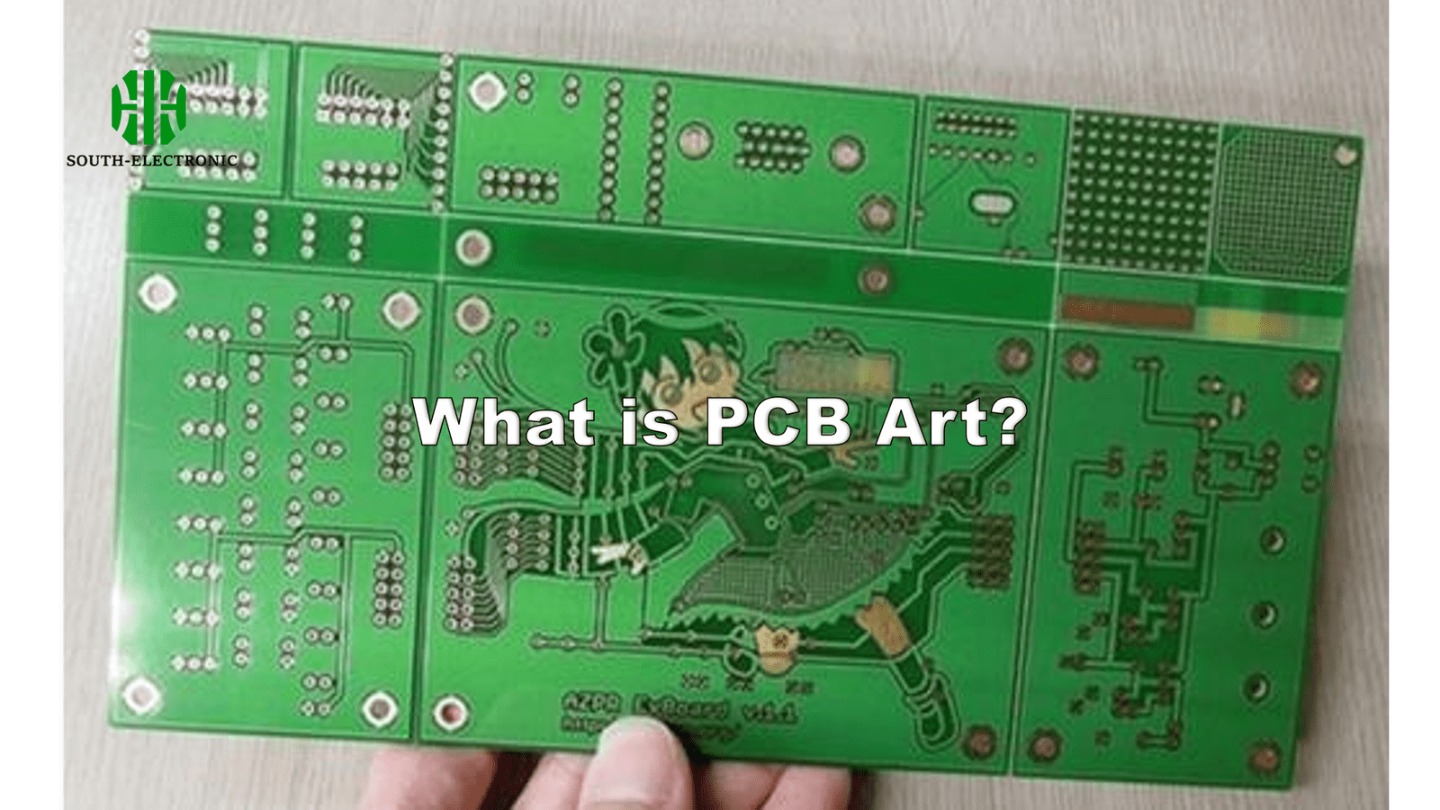
My hands still smell of flux after soldering last night’s project. Beneath the clinical green solder mask lies unexpected beauty – circuit boards have become my canvas for merging engineering precision with artistic vision.
PCB art transforms functional circuit boards into visual storytelling mediums through strategic trace routing, component placement, and solder mask coloring. This emerging discipline bridges electronic engineering with graphic design, turning technical diagrams into collectible artifacts that encode hidden narratives in copper and silicon.
While most see circuit boards as disposable tech components, creators worldwide are revealing their hidden artistic potential. Let’s dissect how cold circuitry becomes warm artistry through four revolutionary dimensions.
Where Electronics Meet Aesthetics – Functional Beauty Redefined
That frustrating EMC compliance test sparked my breakthrough. Forced to reroute problematic traces, I accidentally created a Fibonacci spiral pattern that performed better than my original grid layout.
Modern PCB art[^1] leverages electromagnetic principles[^2] to create functional patterns. Intelligent trace routing balances signal integrity with artistic composition, proving that aesthetic layouts can enhance technical performance rather than compromise it.
)
Three Principles of Aesthetic Circuit Design
| Principle | Engineering Impact | Artistic Application |
|---|---|---|
| Copper Balance | Thermal management | Negative space composition |
| Harmonic Routing | Signal integrity optimization | Geometric pattern creation |
| Layer Synchronization | Crosstalk reduction | Depth perception techniques |
The best PCB artists work like orchestra conductors – aligning technical parameters with visual rhythm. My Xiaomi smartphone tear-down revealed rose-shaped antenna traces that improved 5G reception while creating a floral motif visible under UV light. This dual-purpose design approach challenges the myth that functionality and beauty exist in opposition.
Materials & Techniques Revolution – Beyond Green Soldier Masks
I once ruined a $300 board with nail polish. Today, that mistake evolved into my signature resin-infusion technique[^3] for creating circuit board jewelry.
Contemporary PCB artists employ aerospace-grade materials like translucent PTFE substrates and photo-imageable solder masks[^4]. Gold-plated vias become decorative elements, while UV lasers etch micron-precise illustrations onto copper layers.
)
Material Innovation Timeline
| Era | Key Materials | Artistic Impact |
|---|---|---|
| 1980s | FR-4 fiberglass, green solder mask | Limited color options |
| 2000s | Polyimide flex boards | Curved circuit sculptures |
| 2010s | Transparent aluminum substrates | 3D layered light effects |
| 2020s | Photochromic solder resist | Color-shifting interactive designs |
The shift from industrial-grade to artist-grade materials parallels the steel industry’s transformation during the Art Deco era. My current experiment pairing shape-memory alloys with thermochromic coatings[^5] allows circuits that physically reconfigure and change color when receiving specific signals.
Hidden Meanings in Board Designs – Silicon Semiotics
A client once asked me to encode their family history in a Raspberry Pi case. The resulting board contained Morse code in ground planes and ancestral birthdates in capacitor values.
PCB artists embed symbolic languages[^6] through component selection (resistor color codes), trace geometry (sacred angles), and layer stackups (numerological references). These hidden elements transform circuits into tech-alchemical objects with multiple interpretation layers.
)
Common Cryptographic Techniques
| Method | Technical Purpose | Symbolic Meaning |
|---|---|---|
| Golden Ratio Trace Routing[^7] | Impedance matching | Aesthetic perfection |
| Via Arrays | Heat dissipation | Constellation maps |
| Silk Screen Microtext | Part identification | Poetic verses |
| Capacitor Code Dates | Batch tracking | Historical events |
My favorite "Easter egg" involved designing USB-C breakout boards where the pinout diagram secretly formed Tibetan mandala patterns. These layered meanings create tech artifacts that reward both engineering analysis and philosophical contemplation.
PCB Asthetic Appreciation – Culturing New Perception
I host PCB gallery nights[^8] where engineers examine circuits under microscopes while art students sketch hexadecimal solder joints. The reactions always shatter expectations.
Appreciating PCB art requires understanding three perspectives: functional topology analysis (engineer), compositional balance assessment (designer), and symbolic interpretation (cultural theorist). This tripartite approach reveals the true depth of quality circuitry craftsmanship.
)
Appreciation Criteria Matrix
| Criterion | Technical Metric | Artistic Metric |
|---|---|---|
| Complexity | Signal integrity analysis | Visual hierarchy balance |
| Originality | Patent search | Style differentiation |
| Craftsmanship | IPC class rating | Hand-finishing quality |
| Conceptual Depth | Functional testing | Symbolic coherence |
My recent collaboration with a neurology lab revealed that experienced engineers’ brains activate both analytical and visual cortex areas when viewing exceptional PCB art – literal proof of STEAM education’s cognitive benefits.
Conclusion
Circuit boards evolved from utilitarian slabs to cultural artifacts. PCB art doesn’t just decorate technology – it reveals technology’s inherent beauty, transforming how we perceive engineering itself through creative material alchemy.
[^1]: Explore the fascinating world of PCB art, where technology meets creativity, transforming circuit boards into stunning visual pieces.
[^2]: Understanding electromagnetic principles can enhance your PCB designs, merging functionality with artistic expression.
[^3]: Explore this link to understand how the resin-infusion technique revolutionizes PCB art, turning mistakes into masterpieces.
[^4]: Discover how photo-imageable solder masks are transforming PCB design, allowing for intricate and beautiful patterns.
[^5]: Learn about thermochromic coatings and their innovative applications in electronics, making circuits interactive and visually stunning.
[^6]: Explore how symbolic languages enhance PCB design, adding depth and meaning to electronic art.
[^7]: Learn about the Golden Ratio’s role in PCB design for aesthetic perfection and technical efficiency.
[^8]: Discover the unique blend of art and engineering at PCB gallery nights, where creativity meets technology.


.jpg)