Introduce
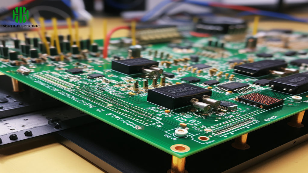
PCB copy is to use reverse research and development technology to reversely analyze the circuit board on the premise that there are already physical electronic products and circuit boards, and convert the original product’s PCB files, bill of materials (BOM) files, and schematic files. Other technical documents and PCB silk screen production documents are restored 1:1, and then these technical documents and production documents are used for PCB board making, component welding, flying probe testing, and circuit board debugging to complete a complete copy of the original circuit board model.
Manufacturing PCB Copy Process
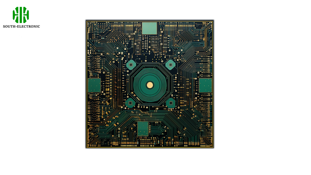
- scanning phase.:Careful inspection under advanced scanning equipment Every trace, pad and via on the PCB is drawn in exquisite detail.
- Reverse engineering stage:Profiling the previously acquired digital map enables engineers to understand the path and component placement of the PCB. .
- Schematic creation stage:Previously deciphered messages were transcribed into comprehensive schematic diagrams. The diagram serves as an architectural plan for the PCB, depicting every connection and component in a clear and concise manner.
- layout design stage:Utilize advanced CAD (computer-aided design) software to convert schematics into physical layouts. This layout reflects the design of the original PCB, ensuring that the copied version functions the same as its original version.
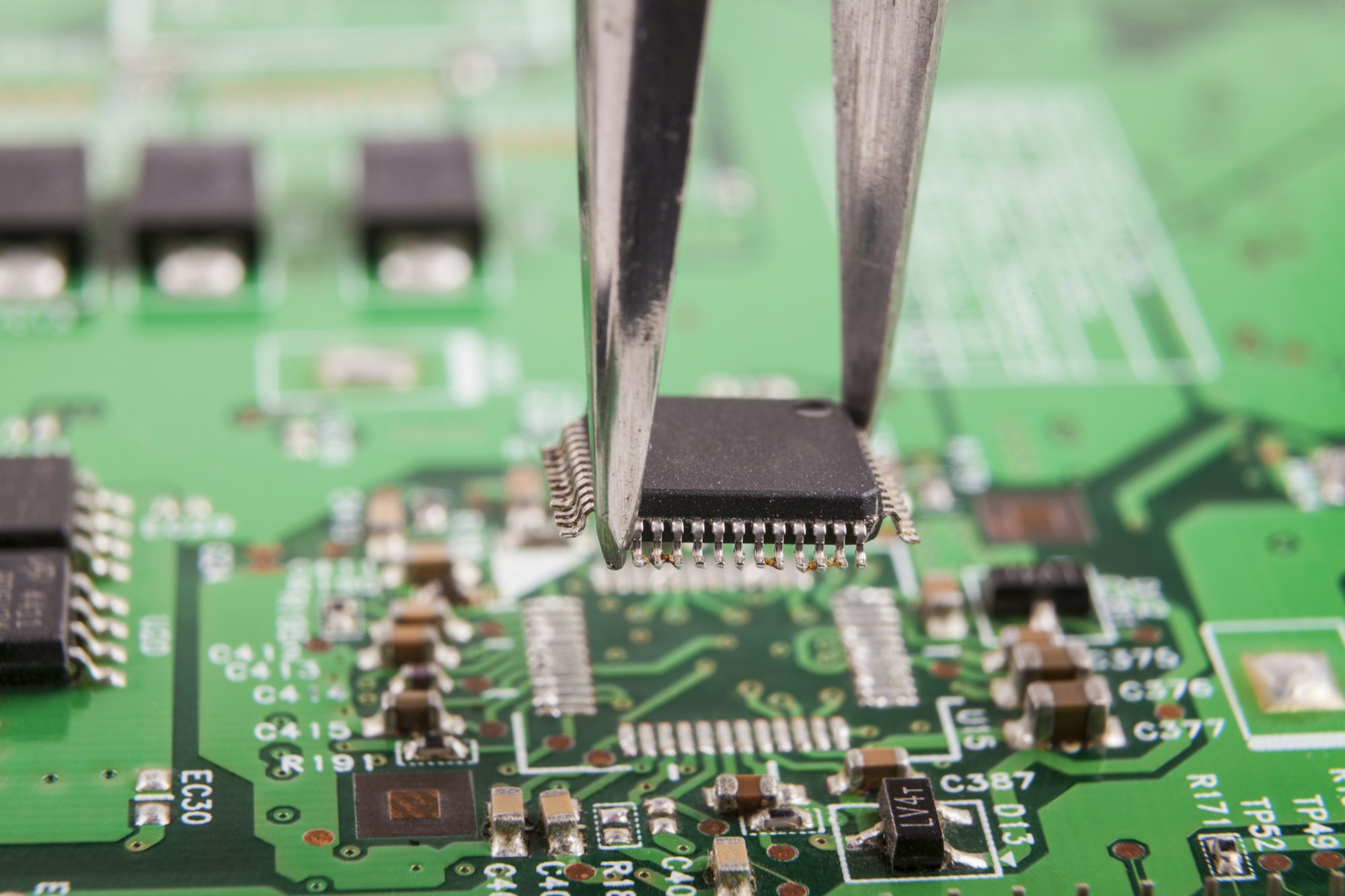
- Manufacturing of PCB copy:The layout serves as a guide to produce the physical circuit board, using high-precision machinery to etch the copper layers, drill through holes, and mount the components, resulting in an exact replica of the original PCB.
- Test and verify:Where newly manufactured PCBs are rigorously tested. The aim is to ensure that it matches the functionality and performance of the original version.

The role of PCB Copy in reverse engineering
It respects the original design through in-depth research and uses this understanding to push the boundaries of what is possible in electronics. When it comes to reverse engineering, PCB copy can be trusted to start by carefully mapping out the entire landscape of the PCB, tracing paths, documenting the location of components, and understanding interconnections. This is not just plagiarism; This is a detailed study, a thorough examination.
PCB copy in reverse engineering is a bridge. It connects the past and present, allowing us to learn from existing designs and apply that knowledge to create something more advanced, efficient or cost-effective.
Quality Control and Testing in PCB Copy
Electrical Testing: The PCB is tested, testing each circuit to make sure they conduct electricity properly.
Functional testing: To ensure that the PCB not only looks good, but also has charm and perfectly reflects the original.
Even the smallest oversight in a PCB can lead to errors, and there are certain requirements for quality control that require rigorous testing to end up with a PCB that works both in form and function.

Conclusion
PCB copy emerges as an extraordinary blend of technology, precision, and innovation. It’s a process that pays homage to existing electronic designs while paving the way for future advancements. Through a series of meticulously executed stages – from scanning, reverse engineering, schematic creation, layout design, to the final manufacturing and testing – PCB copy allows us to create exact replicas of original circuit boards. These replicas are not mere imitations but are functional, high-quality products ready to be utilized in various applications.

