
Custom PCB Fabrication Solutions
Min hole size 4 mil | OSP | HASL | ENIG | FR-4 & High-Frequency | AOI Inspection
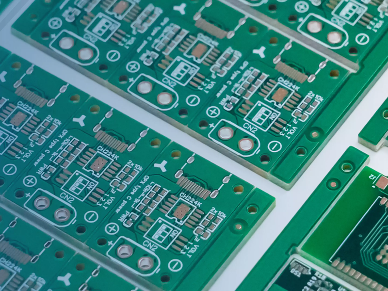
We manufacture high-quality PCBs ranging from 2 to 68 layers, catering to industrial, automotive, and consumer electronics applications. Our commitment to manufacturing excellence ensures stable quality and reliable performance across all production runs.
PCB Fabrication Capabilities
PCB Process Capability
-
Layer Count
8 layers
-
PCB Dimensions
≤24*48inch(610*1220mm)
-
Materials Types
FR-4 | High Tg | Halogen-free | PTFE | Ceramic PCB | Metal substrate material
-
Material Brand
Lianmao|Shengyi| Taiyao| Nanya, Panasonic|Isola|Nelco|Rogers|Taconic|Arlon...
-
Board Thickness
0.2mm-8.0mm
-
Finish Treatment
Immersion Gold|Lead-free HASL|OSP|Immersion Tin|Immersion Silver|Thick Gold Plating|Silver Plating|Immersion Gold+OSP
-
Copper thickness
0.33 OZ-8 OZ
-
SolderMask Color
Green| Blue| Black|Yellow| Red|Purple| White...
-
Finish Treatment
Immersion Gold|Lead-free HASL|OSP|Immersion Tin|Immersion Silver|Thick Gold Plating|Silver Plating|Immersion Gold+OSP
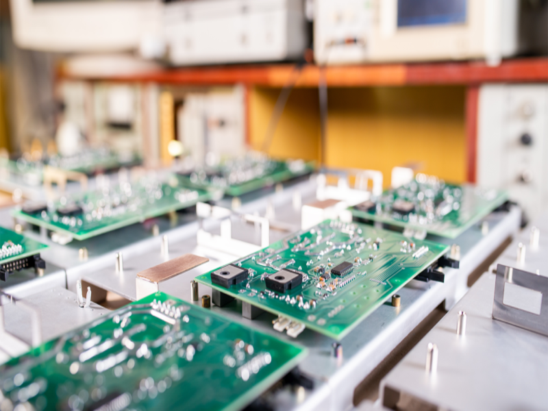
Why Choose Us for PCB Fabrication
We provide engineers with dependable PCB fabrication services,
from initial prototypes to high-volume production runs.
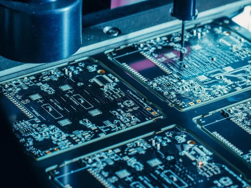
Each PCB undergoes a thorough review by our engineering team to ensure stack-up integrity, impedance control, and manufacturability before production begins.
Our commitment to quality guarantees reliability and performance, whether for prototypes or mass production.
We excel in handling tight tolerances, controlled impedance, and multilayer lamination, making us ideal for intricate PCB requirements.
We prioritize clear communication and prompt responses to support engineering and purchasing teams worldwide.
Related Project We Had Done
PCB Fabrication for Industrial Control System
Application
Industrial Control
Key Specs
Challenge
Result
PCB Fabrication for Industrial Power Control
Application
Key Specs
Challenge
Result
PCB Fabrication for IoT Gateway Device
Application
Key Specs
Challenge
Result
Quality Control & Certifications for PCB Fabrication
Common Questions
Most Popular Questions
What materials are commonly used in PCB fabrication?
How many layers can your PCBs have?
What types of surface finishes do you offer?
How do you ensure quality in PCB fabrication?
Can you handle custom PCB dimensions?
Send Us a Message
The more detailed you fill out, the faster we can move to the next step.
