
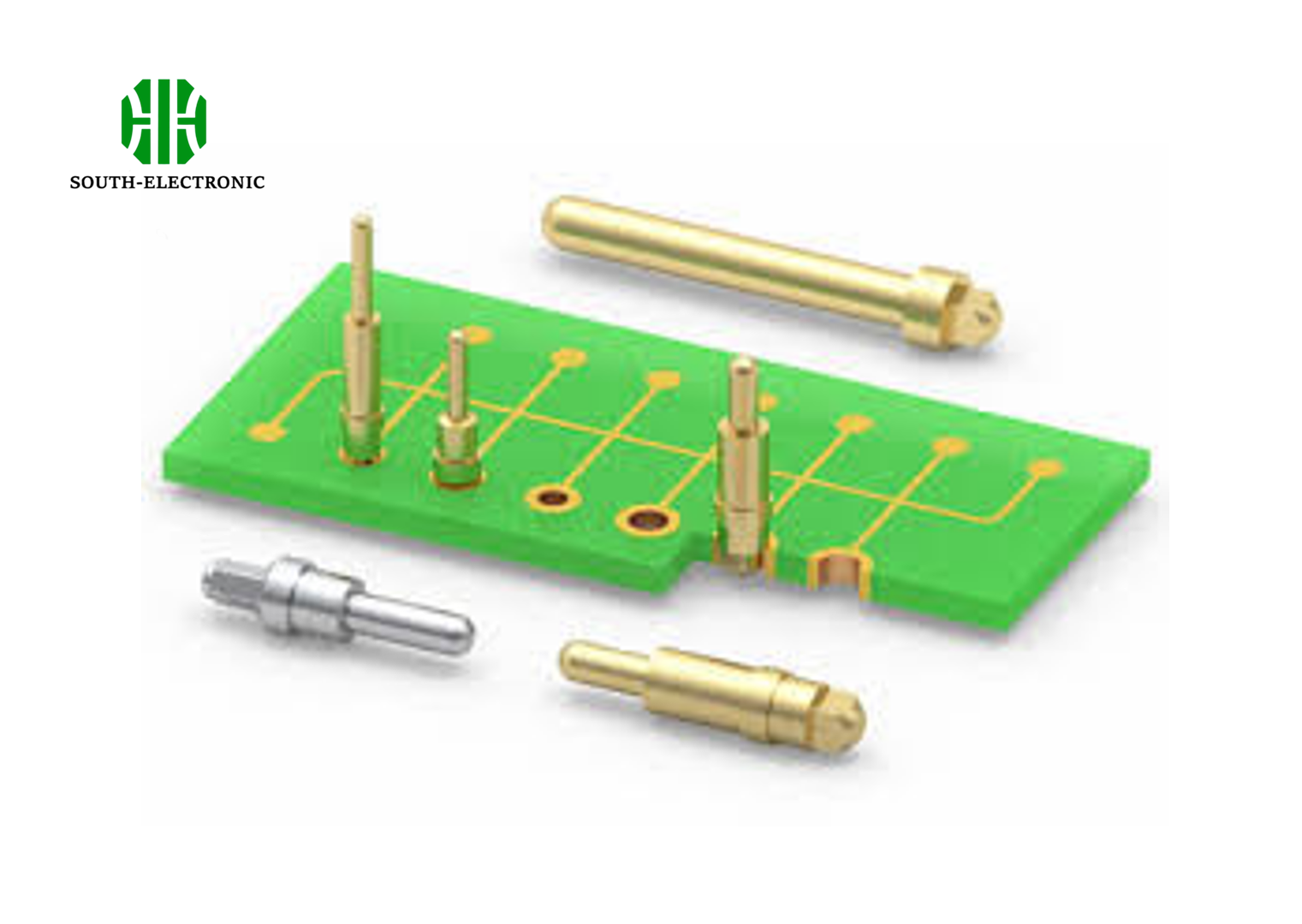
What is a Press-Fit Hole PCB ?
A Press-Fit Hole PCB refers to a printed circuit board (PCB) designed to accommodate press-fit components. These components, such as connectors or other electronic components, are inserted into specially designed holes on the PCB without the need for soldering. The holes are typically plated-through and have a slightly smaller diameter than the pins of the components to ensure a tight fit.

What are the advantages of using press-fit holes in PCBs?
- No Heat Required: Press-fit connections do not require heat, unlike soldering. This avoids potential damage to sensitive components and PCB materials that might degrade under high temperatures.
- Reusability and Repairability: Components fitted with press-fit technology can be easily removed and replaced, facilitating repairs and upgrades without risking damage to the PCB by desoldering and resoldering.
- Reliability: Press-fit connections are highly reliable, especially in environments subjected to mechanical stress and thermal cycling. The absence of solder eliminates issues like cold solder joints or solder flux contamination.
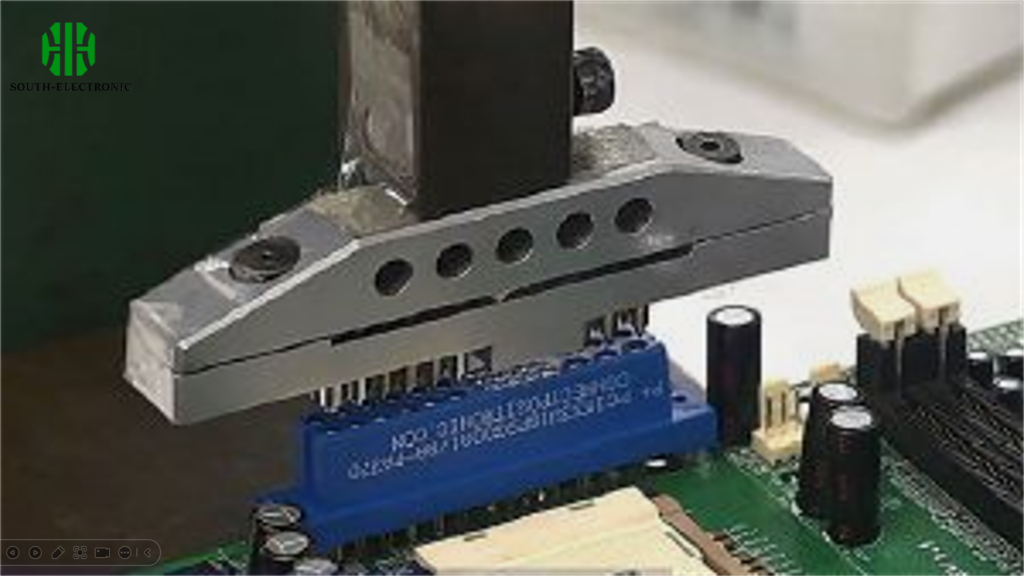
- Faster Assembly: Press-fit components can be inserted mechanically, speeding up the assembly process compared to manual soldering. This is particularly beneficial in high-volume production settings.
- Environmental Considerations: Since there is no need for solder, press-fit technology is free from concerns about lead and other hazardous substances found in some solders, aligning with stricter environmental regulations.
How does press-fit technology differ from soldering in PCB assembly?
Here’s a concise and professional summary of the differences between press-fit technology and soldering in PCB assembly:
- Connection Method: Press-fit uses a mechanical, friction-based insertion of leads into precisely sized holes, while soldering involves creating a bond by melting a metal alloy around the component leads.
- Thermal Impact: Press-fit does not involve heat, avoiding potential thermal damage to components and PCBs, unlike soldering which exposes them to high temperatures.
- Mechanical Stress: Press-fit connections are more robust against mechanical stresses and are ideal for environments with vibrations or impacts, unlike soldered joints which can be more fragile.
- Ease of Modifications: Components can be easily removed and replaced in press-fit assemblies without damaging the PCB, a process more complex and potentially harmful with soldering due to the need for reheating.
- Skill and Equipment Requirements: Press-fit can be more easily automated and requires less specialized skill compared to soldering, which needs skilled operators and specific tools like soldering irons and reflow ovens.
Types of Holes in PCBs
Characteristics of Different Types of PCB Holes:
| Hole Type | Application | Advantages | Typical Dimensions |
| Plated Through Hole (PTH) | Via Holes | Provides strong electrical connections across layers; durable. | Diameter: 0.6 mm – 1.0 mm |
| Non-Plated Through Hole (NPTH) | Used for mechanical fixtures like screws. | Suitable for non-electrical components; avoids unnecessary conductivity. | Diameter: 0.8 mm – 1.2 mm |
| Blind Hole | Via Holes | Connects surface layers to internal layers without going through the entire board; enhances density without compromising space. | Diameter: 0.3 mm – 0.6 mm |

What are some tips for designing effective press-fit holes in PCBs?
| Tip | Description |
| Accurate Hole Dimensions | Ensure the hole dimensions are precise to maintain a tight fit without excessive force or looseness. |
| Plated Through-Holes | Use plated through-holes to enhance the electrical connection and mechanical strength. |
| Consider Tolerances | Account for manufacturing tolerances to ensure consistent fit across all components and boards. |
| Material Consideration | Choose board materials that can withstand the mechanical stress without cracking or deforming. |
| Test Assembly | Prototype and test the press-fit connections before full-scale production to ensure reliability. |
| Support Around Holes | Design the layout to provide adequate support around holes to prevent damage during component insertion. |
| Clearance Checks | Ensure there is enough clearance around the holes for component leads without causing shorts. |
How does press-fit technology impact the overall cost of a PCB assembly?
Press-fit technology can reduce the overall cost of PCB assembly by minimizing the need for skilled labor and expensive soldering equipment. It simplifies the assembly process, reduces errors and associated waste, and enhances product reliability, potentially lowering long-term service and warranty costs. While the initial setup for press-fit may be pricey, the savings on labor, equipment, and compliance with environmental regulations often make it a cost-effective choice, especially beneficial in high-volume productions.

